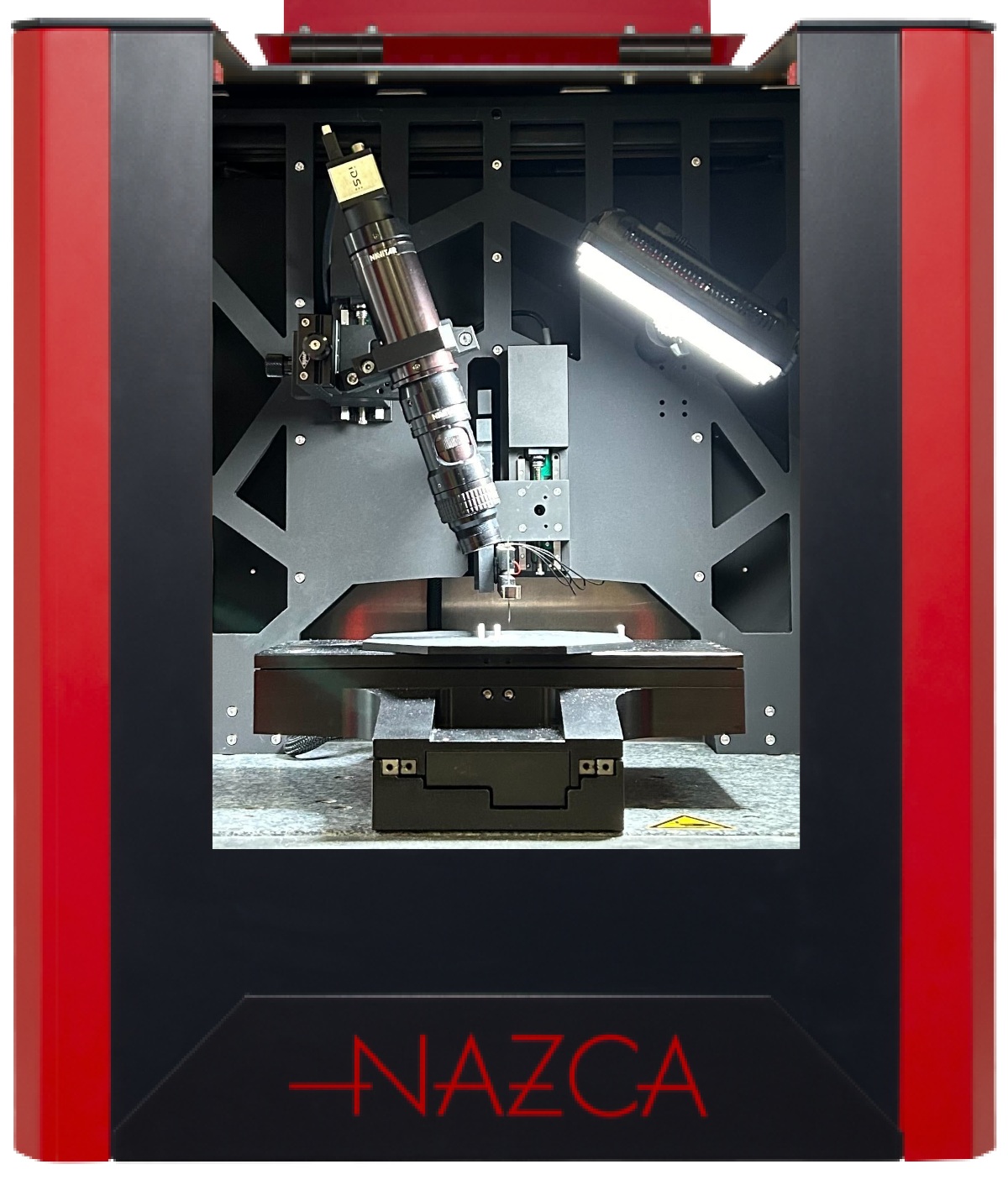
High Precision Capillary Printing (HPCaP)
High Precision Capillary Printing (HPCaP) is an additive printing method developed by Hummink. It prints conductive, polymer and quantum dot inks in lines from about 75 µm down to 500 nm wide, on rigid or flexible substrates, without masks or UV exposure. SiSTEM supplies Hummink’s NAZCA printer in the UK, Ireland, the Nordic countries, Germany, Austria and Switzerland.
How HPCaP works
The printing tip is a glass or quartz pipette filled with ink, mounted on a resonator that oscillates at a set frequency. The method comes from atomic force microscopy. As the pipette approaches the substrate, the ink meniscus touches the surface and the resonance changes, which tells the system it has made contact. From then on, capillary force alone draws the ink out of the pipette as the stage moves, and the electronics hold the pipette at the right height so it follows the surface.
The pipette tip sets the line width. Quartz pipettes from 300 nm to 700 nm print the finest lines, from about 500 nm, and glass pipettes from 1.5 µm to 50 µm print wider ones, up to about 75 µm. A line comes out roughly 1.2 to 1.6 times the tip diameter, depending on the ink and the surface.
How it compares with other printing methods
Inkjet fires droplets at the surface. That limits it to thin inks, around 50 cP by Hummink’s figures, and can leave splashes and satellite drops. HPCaP deposits ink by contact, so nothing is ejected, and it prints inks up to 100,000 cP.
Photolithography still makes the finest features in volume. For prototypes, small batches and repairs, HPCaP takes out the mask and the etch, because the pattern goes straight from a drawing file to the substrate.
Where HPCaP is used
Printed electronics and sensors. Duke University printed carbon nanotube transistors with 500 nm gaps between the electrodes. Université Paris Cité’s ITODYS laboratory uses NAZCA to print transistor-based biosensors, and ONERA, working with Hummink, has printed electrodes on MEMS vibrating gyroscopes.
Display and semiconductor repair. Defects under 5 µm cause a large share of display panel losses, and HPCaP prints silver lines below 5 µm to repair them. It also prints quantum dots locally to repair pixels and build colour conversion layers. In semiconductor packaging it repairs open defects and prints silver microbumps in one step.
Photonics. Hummink and the Karlsruhe Institute of Technology printed an SU8 grating with a 370 nm pitch directly on glass for a perovskite DFB laser. With CEA-Leti, Hummink printed thin polymer masks to pattern transparent conductive oxide films deposited by ALD.
Decoration on delicate surfaces. HPCaP prints fine detail on fragile substrates such as sapphire, and Hummink has applied it to luxury watch dials.
Questions we’re often asked
What’s the smallest line HPCaP can print? About 500 nm, using a 300 nm quartz pipette. The exact width depends on the ink and the surface.
Which inks can I use? Hummink’s own metal and polymer inks, and other inks up to 100,000 cP such as UV resist and quantum dot inks.
Can I see it print my design first? Yes. We can arrange a demonstration or sample prints on your own substrate. Contact us to set it up.