

- Bright light macro inspection for 50mm to 200mm wafers
- Up to four light types, each chosen for a defect type
- Auto and manual modes run from engineer recipes
- Tabletop footprint of 45″ x 34″
Optical Defect Inspection
Optical defect inspection uses light to find defects on a wafer surface before they’re carried further down the line: particles, scratches, resist striations, stepper focus spots, drips and chuck marks. SiSTEM supplies C&D Semiconductor’s inspection systems, which cover bright light macro inspection, combined macro and microscope defect review, and automated wafer loading for an existing microscope.
Macro inspection under bright light
Many lithography defects show up faster under bright light than under a microscope. In macro inspection the operator looks at the whole wafer, tilting and turning it under light chosen to make a particular kind of defect stand out. Wafers that pass go back to the line, and anything suspicious goes on to the microscope.
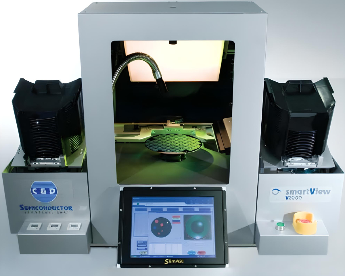
The C&D V2000 holds each wafer on a three-axis gimbal chuck inside a light-controlled housing, for wafers from 50mm to 200mm. It takes up to four light types, each matched to a defect:
- Line light: collimated high-angle light for surface particles
- Bright light: resist striations
- Pink monochromatic light: small stepper focus spots
- Green monochromatic light: photoresist drips
- Bright LED topside light: die damage from process tools
- Soft pink neon light: spin chuck marks and particles
Engineers write the recipes and operators run them in auto or manual mode. C&D reports customers cutting microscope inspection in the lithography area by up to 90% with it. For 300mm wafers, C&D builds the same inspection on its S5030 platform.
Macro and microscope review on one system
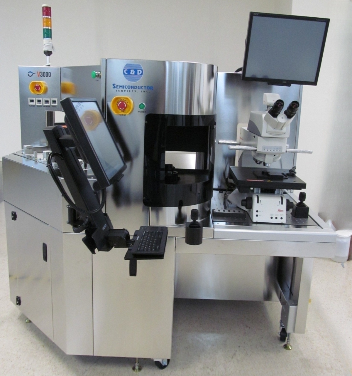
The C&D V3000 puts both stages of the review on one tool, for wafers from 50mm to 300mm. After alignment and OCR, the robot takes each wafer to a bright light station with up to six light sources, where the operator marks every defect on a touchscreen. The wafer then moves to a Leica DM8000 microscope, and the motorised stage brings each marked defect under the objective. The system stores every defect’s location and image against the wafer ID, and results can be exported in KLARF format.
Loading an existing microscope
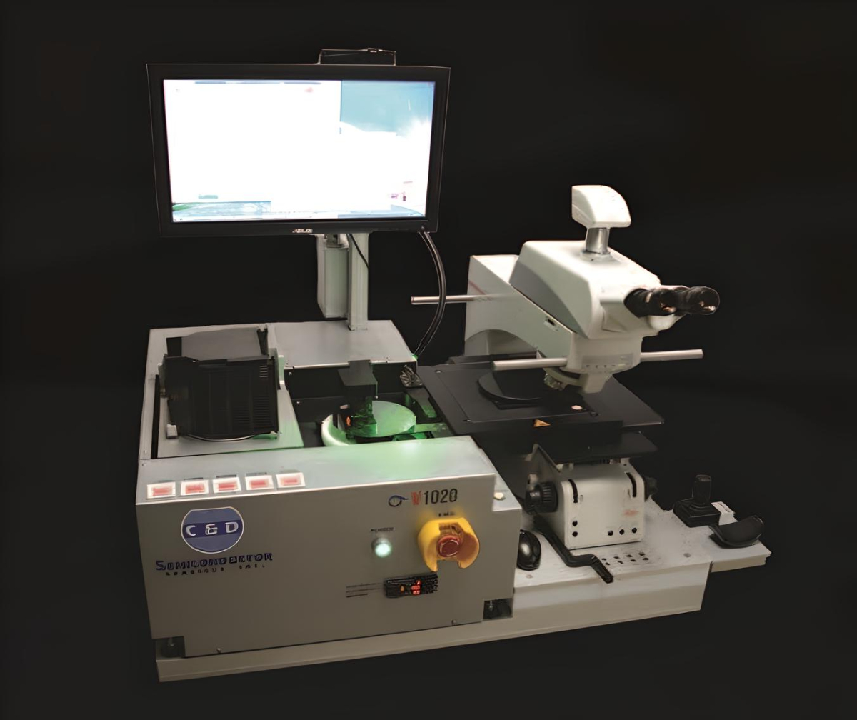
The C&D V1020 moves wafers from the cassette to the microscope stage and back, so the operator only has to inspect. While one wafer is under the microscope, the next is centred and aligned, then given a top and backside macro check at an intermediate station. It works with most microscopes, and C&D rates it at more than 200 wafers an hour.
Optical defect inspection questions
What is optical defect inspection?
Inspecting a wafer surface with light, by eye or through a microscope, to find particles, scratches, residues and process marks before the wafer moves on.
What’s the difference between macro and micro inspection?
Macro inspection looks at the whole wafer at once under bright light and finds defects visible at wafer scale. Micro inspection uses a microscope at high magnification to review individual defects, usually the ones macro inspection has marked.
Do these systems find defects automatically?
They’re operator-led. The operator finds and marks each defect, and the system records its location and image against the wafer ID.
Which wafer sizes do they handle?
The V2000 and V1020 take 50mm to 200mm, and the V3000 takes 50mm to 300mm. For 300mm bright light inspection, C&D builds the S5030.
Buying through SiSTEM
SiSTEM is C&D Semiconductor’s distributor for the UK and Ireland, and we’re glad to hear from customers further afield too. We specify each system with you and C&D’s engineers, then quote and supply it, and our after-sales team installs and supports it. If a tool goes down, we stay on the fault with C&D until you confirm it’s working properly again. Get a quote, or contact us with your wafer sizes and the defects you need to find.
Optical Defect Inspection Products
-
V2000 Bright Light Inspection System
-
V3000 Macro-Scope Defect Review System
- Macro and microscope defect review on one system
- 50mm to 300mm wafers, dual cassette
- Up to six light sources and a Leica DM8000 microscope
- Defect images and classification stored by wafer ID
-
V1020 Microscope Wafer Loader
- Loads wafers from cassette to microscope stage and back
- 50mm to 300mm, with auto detection of two wafer sizes
- More than 200 wafers an hour
- Fits most microscopes