- Advanced PVA brush technology for post-CMP cleaning
- Designed for contamination reduction and low defectivity
- Effective removal of slurry residue and metallic contaminants
- Controlled pore structure for highly consistent cleaning performance
- Integrated brush-core design for enhanced process stability
- Compatible with advanced semiconductor packaging applications
- Available for multiple wafer sizes and cleaning platforms
Email: info@sistemtechnology.com Call: +44 (0)1327 362 844
Post-CMP Cleaning Solutions for Semiconductor Manufacturing
Post-CMP cleaning is one of the most critical stages within semiconductor manufacturing, directly impacting wafer cleanliness, process stability, device reliability and overall production yield.
Following Chemical Mechanical Planarisation (CMP), residual slurry particles, metallic contaminants and organic impurities must be effectively removed from wafer surfaces to prevent defects and ensure consistent downstream processing.
As semiconductor devices continue to shrink and advanced packaging technologies become increasingly complex, contamination control requirements within post-CMP cleaning environments have become significantly more demanding.
SiSTEM Technology supplies advanced semiconductor cleaning technologies and consumables designed to support highly controlled wafer cleaning processes across research, development and semiconductor manufacturing environments.
Why Post-CMP Cleaning Matters
CMP processes are essential for achieving highly planar wafer surfaces required for advanced semiconductor device fabrication. However, the polishing process can leave behind microscopic contamination including abrasive slurry particles, metallic residues, organic contaminants and surface defects.
Even extremely small levels of contamination can negatively impact:
• Wafer yield and process consistency
• Device reliability and long-term performance
• Thin film integrity and bonding quality
• Advanced packaging processes
• Downstream lithography and deposition stages
Advanced Contamination Control Technologies
Modern semiconductor manufacturing environments require increasingly sophisticated cleaning technologies capable of delivering highly consistent, low defectivity wafer cleaning performance.
Advanced post-CMP cleaning solutions are designed to support:
• Slurry residue removal
• Metallic contamination reduction
• Organic defect control
• Surface particle removal
• Low defectivity cleaning
• Stable process repeatability
• Improved yield performance
Supporting Advanced Semiconductor Manufacturing
As semiconductor technology continues advancing towards smaller geometries, heterogeneous integration and advanced packaging, post-CMP cleaning performance becomes increasingly important throughout the manufacturing process.
Applications increasingly reliant on advanced contamination-control technologies include:
• FEOL, MOL and BEOL processing
• Advanced semiconductor packaging
• HBM manufacturing
• Hybrid bonding
• Photomask cleaning
• Wafer reclaim and substrate cleaning
• MEMS and micro-sensor manufacturing
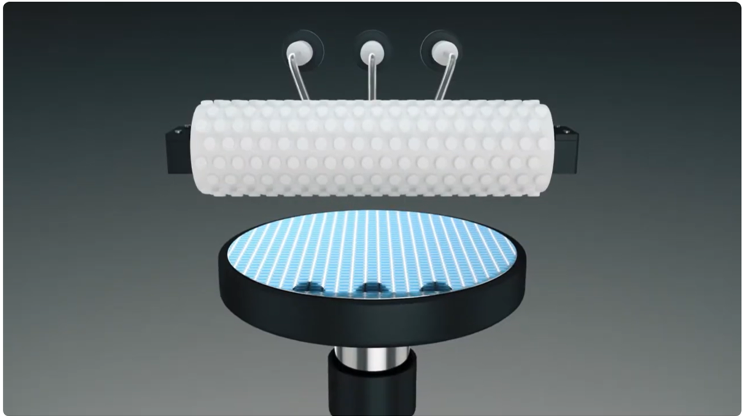
Purience PVA Brush Technology
SiSTEM Technology supplies advanced Purience PVA brush technologies designed specifically for demanding post-CMP semiconductor cleaning environments.
Purience technologies utilise highly hydrophilic PVA structures, controlled pore architectures and integrated brush-core designs to support highly consistent wafer cleaning performance while minimising particle generation and surface damage risks.
These advanced consumables are developed to support contamination reduction, process stability and yield improvement across advanced semiconductor manufacturing environments.
Discuss Your Post-CMP Cleaning Requirements
SiSTEM Technology supports semiconductor customers across Europe with advanced wafer cleaning technologies, contamination-control consumables and process expertise for post-CMP semiconductor manufacturing applications.
Contact our team to discuss your process requirements, wafer sizes, equipment compatibility and application challenges.