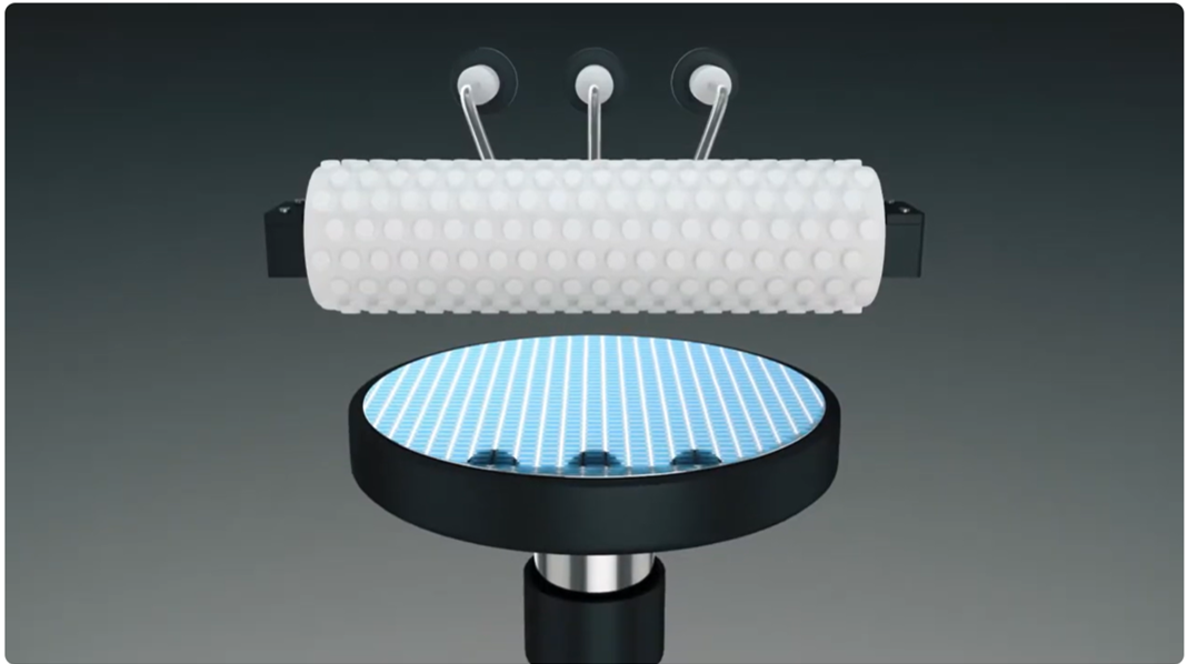
PVA Brush for Post-CMP Semiconductor Cleaning
Purience PVA Brush for Post-CMP Semiconductor Cleaning
Purience PVA brushes are high-performance semiconductor cleaning consumables designed for post-CMP wafer cleaning applications. Engineered for contamination control, process stability and low defectivity, they support the removal of residual slurry particles, organic impurities and metal contaminants from wafer surfaces after CMP processing.
With a highly hydrophilic PVA structure, interconnected pores and advanced brush-core design, Purience PVA brushes are developed to meet the strict cleanliness requirements of semiconductor manufacturing, including FEOL, MOL, BEOL and advanced packaging processes.
Purience also develops next-generation brush technologies focused on organic contamination reduction, metal cross-contamination control, improved planarity and enhanced process consistency for advanced semiconductor manufacturing environments.
Key Benefits
- Designed for post-CMP wafer cleaning and contamination control.
- Supports removal of slurry residue, particles, organic impurities and metal contaminants.
- Highly hydrophilic PVA structure with interconnected pores.
- Non-linting and non-scratching for sensitive semiconductor surfaces.
- High water absorption and controlled pore structure.
- Integrated core-brush structure for improved cleaning stability.
- Suitable for advanced wafer processing and packaging applications.
Outstanding Features
- Rigid when dry and soft when wet
- Highly resistant to a range of acids, bases and organic solvents
- Mechanically strong and abrasion resistant
- Controlled pore size and pore distribution
- Heat resistant up to 80°C in wet conditions
- Designed to reduce dust generation and surface scratching
- Available for 200mm and 300mm wafer cleaning applications
Typical Applications
- Post-CMP cleaning for FEOL, MOL and BEOL processes
- Advanced semiconductor packaging
- HBM and hybrid bonding process support
- Photomask cleaning
- Substrate reclaim and wafer cleaning
- Critical thin film cleaning, including nano-coating and smart glass applications
- Micro sensor and advanced technology cleaning applications
Product Configurations
Purience PVA brushes are available in multiple configurations to support different wafer sizes, process tools and cleaning requirements. Standard product families include 200mm and 300mm PVA brush formats, with options developed for compatibility with major post-CMP cleaning platforms.
Available formats include roll-type, disk-type and pencil-type PVA brushes, allowing the technology to be matched to the specific cleaning process and equipment configuration.
Technical Properties
- 200mm brush median pore size: approximately 60–80 µm
- 300mm brush median pore size: approximately 70–120 µm
- Porosity: approximately 88–90% depending on configuration
- Water absorption: approximately 750–1000% depending on configuration
- Low density PVA structure designed for effective wet cleaning performance
Chemical Resistance
Purience PVA brushes are designed for compatibility with a range of common semiconductor cleaning chemistries, including selected acids, bases and organic solvents. This supports use within demanding post-CMP cleaning environments where chemical resistance, cleanliness and process stability are essential.
Advanced Brush Technology
Purience’s technology roadmap includes integrated brush development, advanced pore control, selective contamination removal and surface charge control. These developments are focused on reducing organic contamination, minimising metal cross-contamination and improving cleaning consistency for advanced semiconductor nodes and packaging technologies.
SiSTEM Technology can support customers with Purience PVA brush selection for post-CMP cleaning applications, including discussion of process requirements, wafer size, equipment compatibility and evaluation opportunities.