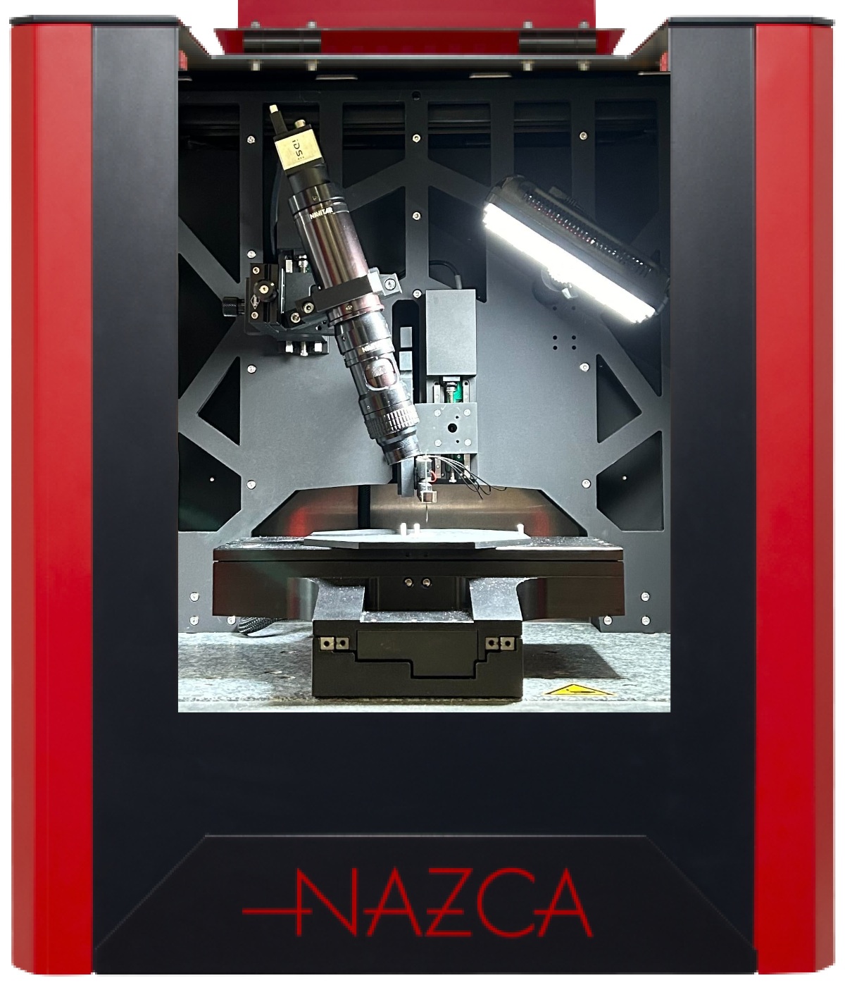
Hummink: High Precision Capillary Printing (HPCaP)
Hummink is a Paris company that makes equipment and inks for printing at the micron and sub-micron scale. Its printing method grew out of atomic force microscopy research at the École Normale Supérieure, PSL University, CNRS and the Institut Pierre-Gilles de Gennes. The first patent was filed in 2018 and the company was founded in 2020.
The method is High Precision Capillary Printing (HPCaP). A glass or quartz pipette filled with ink oscillates just above the surface, and when its meniscus touches down, capillary force draws the ink out as the stage moves. It works without masks or UV exposure, so a pattern goes straight from a drawing file to the substrate. Hummink’s research printer is the NAZCA, which prints lines from about 75 µm down to 500 nm wide. Hummink also makes its own inks and pipettes, and works with manufacturers on building HPCaP into their own production equipment.
SiSTEM Technology is Hummink’s distributor for the UK, Ireland, Denmark, Norway, Sweden, Finland, Iceland, Germany, Austria, Switzerland and Liechtenstein. We quote and supply NAZCA printers and consumables, arrange demonstrations and sample prints on your own substrates, and support installation and training with Hummink’s engineers. We’ve supplied NAZCA printers to the University of Southampton and to DTU in Denmark. Contact us to talk through what you’d like to print.