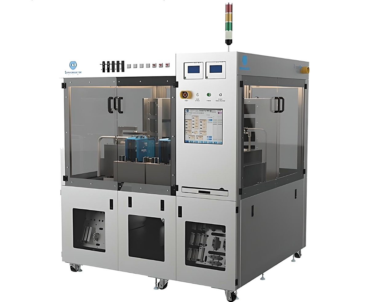
P9000 Wafer Processing Cluster System
C&D Semiconductor P9000 Wafer Processing Cluster System
The C&D Semiconductor P9000 Wafer Processing Cluster System is the pinnacle of innovation in photoresist coating and development, catering to the versatile needs of semiconductor fabrication. Engineered to handle substrates ranging from 50mm to 300mm, the P9000 stands as a testament to flexibility and efficiency in the semiconductor industry. This wafer processing system is meticulously designed to accommodate an extensive selection of modules, including various photoresist coaters, developers, vapour prime modules, hot plates, and chill plates, alongside specialised process modules that incorporate cutting-edge technologies like optical centering and edge bead removal.
With an emphasis on adaptability, the P9000 Cluster System offers unparalleled throughput capabilities within its remarkably compact design. It’s capable of being tailored as a coater, developer, vapour prime, bake, chill unit, or any combination thereof, catering to a broad spectrum of photoresist spin coating and photosensitive polymer applications. C&D Semiconductor’s specialisation in custom photoresist coaters allows for optimisation tailored to specific customer needs, enhancing efficiency and minimising costs. The system’s design enables a reduction in the cluster system’s footprint to accommodate even the most critical spatial constraints within a fab environment. Furthermore, the P9000 Wafer Processing Cluster System facilitates future growth with options for expansion bays, allowing for the addition of modules or adaptation to larger substrate sizes in response to evolving project requirements.
The P9000 Cluster System is at the forefront of technological advancement, featuring state-of-the-art innovations such as ultrasonic spray coating, the revolutionary Synchrospin coating system, and optical enhancements for traditional modules, including Optical Edge Bead Removal (OEBR) and Optical Centering. These features underscore C&D Semiconductor’s commitment to pushing the boundaries of what’s possible in semiconductor processing technology.
Key Benefits
- Exceptional flexibility with stacked module design.
- Compact footprint to maximise cleanroom space.
- High-performance brushless motors ensure outstanding uniformity and reliability.
- Precise edge bead removal for impeccable substrate processing.
Outstanding Features
- Compatibility with 50 mm to 300 mm substrates.
- Central atmospheric robot equipped with a dual-end effector for efficient handling.
- User-friendly PC Windows-based operating system with smartPro GUI for intuitive control.
- Compliance with industry standards: CE Mark, and SEMI S2, S6, S8, and S10 certifications.
- HEPA filtered
Customisable Options
- Integrated chemical cabinets for safe material storage.
- Syringe dispense systems for precise material application.
- Remote chiller support for temperature-sensitive processes.
- Advanced environmental controls for optimal processing conditions.
- Exhaust and fire suppression systems for enhanced safety.
- SECS/GEM compliance for seamless integration into existing manufacturing systems.
- Ability to run three different wafer sizes without the need for hardware modifications.
- Barcode and recipe download capabilities for streamlined operation.
The C&D Semiconductor P9000 Wafer Processing Cluster System is not just equipment; it’s a comprehensive solution designed to meet the dynamic demands of semiconductor manufacturing, promising to enhance efficiency, reduce operational costs, and pave the way for future innovations.
Wafer Processing Modules
Coater Module
- Interface: Windows-based PC with touchscreen panel
- Dispense Arm Action Range
- Static – x axis (programmable)
- Dynamic – x axis (programmable)
- Vertical – Z axis (programmable)
- PR Dispense Arm Nozzle: High resolution 5-phase stepping motor with microstepping driver
- No. of Dispenses: Up to five (5) dispenses
- Spindle Spin Method: AC brushless servo motor with controller, 10 – 8,000 RPM, 50K Acceleration
- Spin Increment: 1 RPM
- Top EBR: Separate arm for Top EBR. Programmable (0.10 mm increments better)
- Bottom EBR: Bottom EBR built-in catchup
- Spin Cup Spec: Low turbulence, built-in vapour curtain dunker, metered solvent. Optional self-cleaning catch cup. Separate exhaust & fluids in process cup
- Environment: Optional temperature, humidity and air flow control
Developer Module
- Dispense Arm Action Range
- Static – x axis (programmable)
- Dynamic – x axis (programmable)
- Vertical – Z axis (programmable)
- DI Rinse: Stationary low impact stream, optional DI water spray
- Developer Solutions: Up to four (4)
- Spindle Spin Method: AC brushless servo motor with controller, 10 – 8,000 RPM, 50K Acceleration
- Spin Increment: 1 RPM
- Environment: Optional temperature, humidity and air flow control
Alloy
- Temperature Range: 50ºC to 500ºC
- Method: Atmospheric chamber/Special chamber for gases and nitrogen
Vapour Prime
- Temperature Range: 25ºC to 190ºC
- Method: Programmable and/or fixed proximity bake capability
Chill Plate
- Temperature Range: Controlled temp from ambient to 15ºC with optional chiller
Hot Plate
- Temperature Range: Ambient to 300ºC
- Temperature Uniformity
- +/-1.0% across the wafer (open hotplate)
- +/-0.5% across the wafer (closed lid)
- Temperature Rise/Time
- From ambient to 150ºC stable temp – 10 min max
- From ambient to 300ºC stable temp – 20 min max
- Temp Display: Digital controller