

- Coat, develop, bake, prime and chill modules in any mix
- 50mm to 300mm wafers, up to three sizes without hardware change
- Spray coating, metal lift-off, alloy and optical EBR options
- Built in San Jose, supplied and supported by SiSTEM

C&D Semiconductor Wafer Processing Systems
C&D Semiconductor Services designs and builds wafer processing and inspection equipment in San Jose, California, where it was founded in 1989. Its two process platforms, the P9000 cluster tool and the P8000 linear track, carry photoresist coat and develop, bake, vapour prime, wafer scrubbing, metal lift-off and alloy modules for wafers from 50mm to 300mm. Alongside them sit the P7000 alloy-anneal system, the V-series inspection tools and the S5000 wafer sorter. C&D has more than 1,500 systems installed worldwide, in R&D labs, pilot lines and high-volume fabs.
SiSTEM is C&D’s distributor for the UK and Ireland, and we’re glad to hear from customers further afield too. We specify each system with you and C&D’s engineers, then quote and supply it, and our UK and European after-sales team installs it and looks after it. Contact us to talk through your process, or see the systems below.
Built in San Jose since 1989
C&D designs and builds every system in San Jose, with its own machine shop and software team, so hardware and software can be changed to suit a process.Coat, develop and bake
Positive and negative resists, thick films up to 150 µm, polyimide, BCB and spin-on glass, with aqueous or solvent developers, optical edge bead removal and LED flood exposure.Lift-off and wafer cleaning
Heated-solvent metal lift-off and resist strip with dry-in, dry-out handling, plus high-pressure and brush scrubbing. Wafers on tape frames can be coated and cleaned before and after dicing.Alloy and anneal up to 500°C
Single-wafer metal alloy and low-temperature anneal in a controlled gas atmosphere, for ohmic contacts on GaAs, InP, GaN and SiC. C&D builds it as a lower-cost route than rapid thermal annealing.Inspection and wafer handling
Bright light macro inspection, combined macro and microscope defect review, automated microscope loading, and wafer sorting with front and back OCR.From research wafers to production
The same platforms run 50mm research wafers and 300mm production lines, on silicon, compound semiconductors, glass and lithium niobate.Products from C&D Semiconductor
-
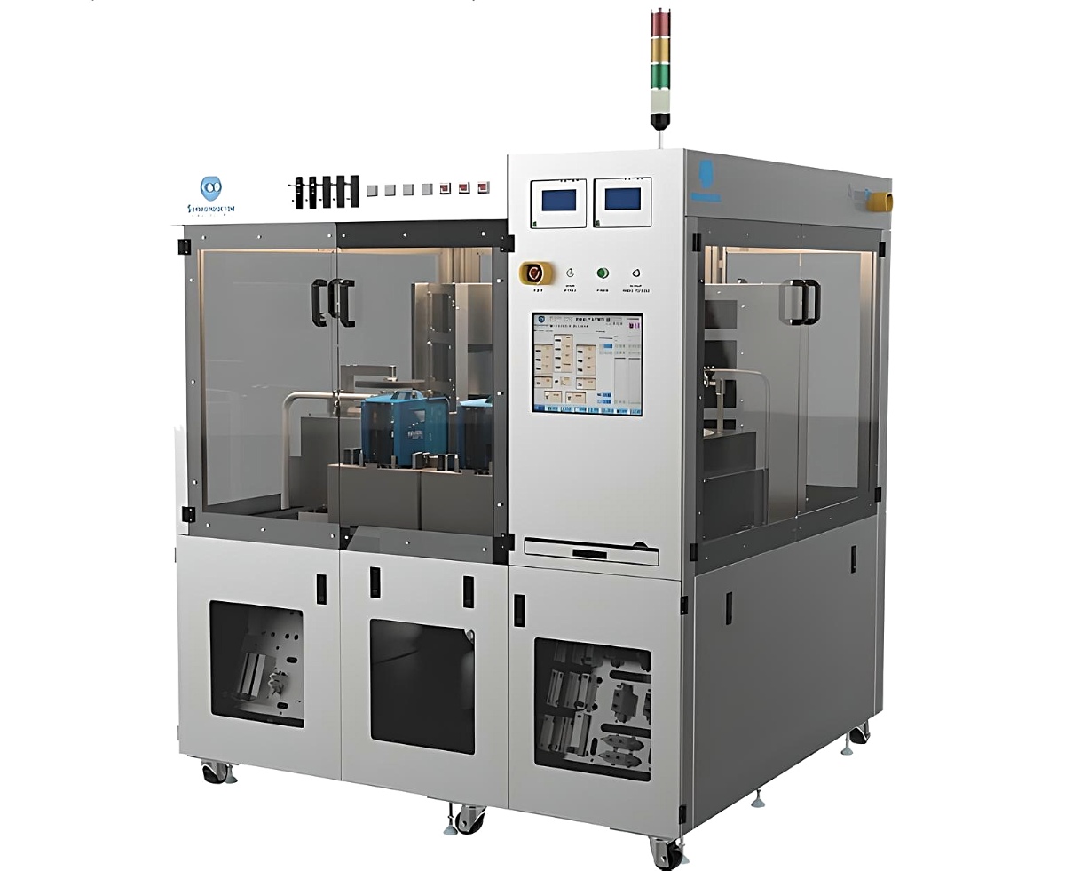
P9000 Coat and Develop Cluster Tool
-
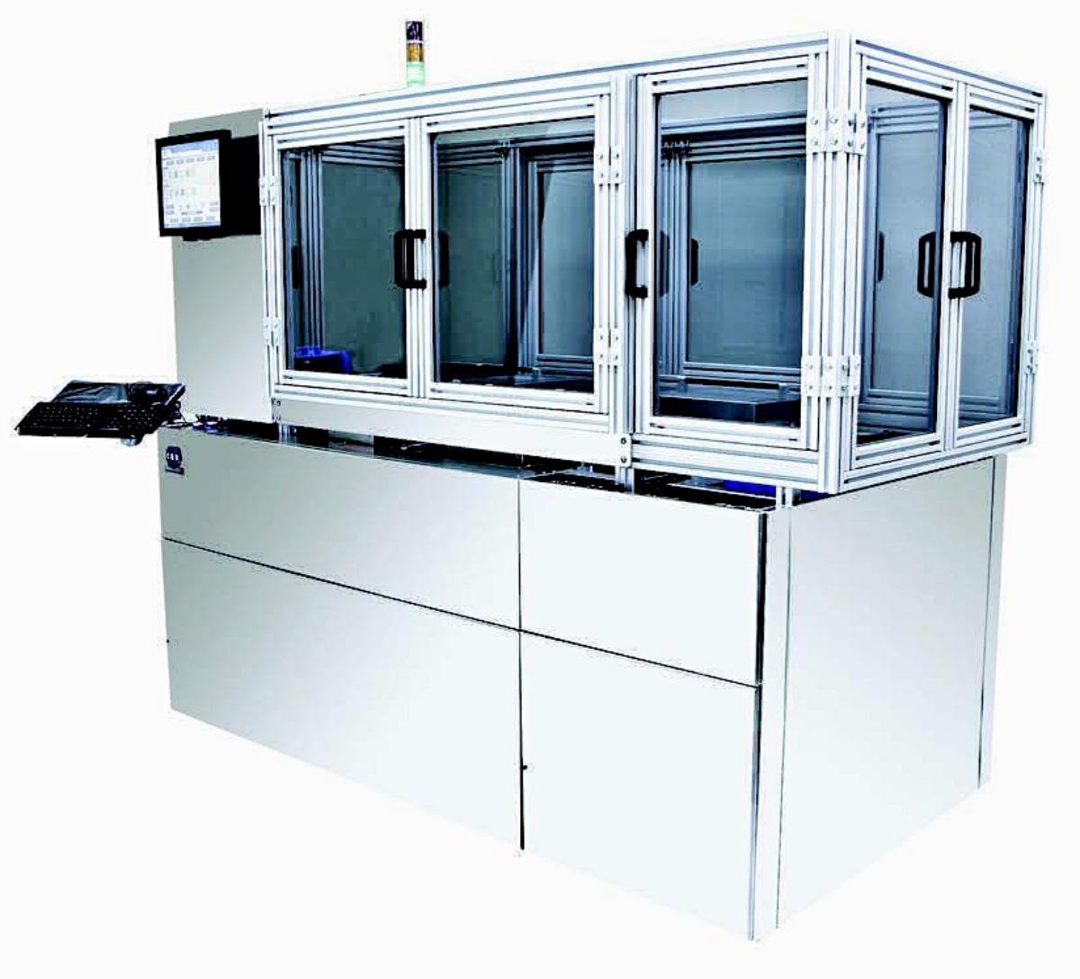
P8000 Linear Coat and Develop Track
- Linear coat and develop track for 50mm to 200mm wafers
- Coater, developer, hot plate, chill, vapour prime and scrubber modules
- Built new, with obsolete parts designed out
- Built in San Jose, supplied and supported by SiSTEM
-
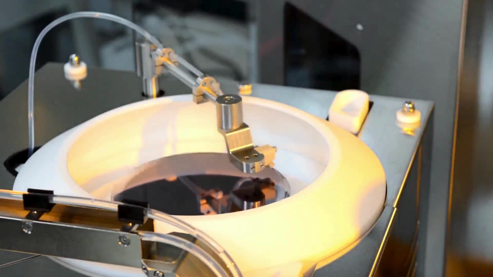
Metal Lift-Off System
- Solvent soak and high-pressure spray lift-off in one module
- Dry-in, dry-out, cassette to cassette
- Heated acetone, IPA, NMP and other solvents
- Separate drains for metal recovery
-
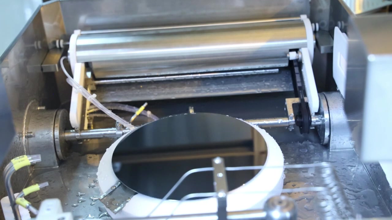
Wafer Scrubber and Cleaning System
- Roller brush and high-pressure spray cleaning
- Wafers, grinding carriers and mask blanks
- 100mm to 300mm, one to four scrubber modules
- Dry-in, dry-out, with two chemistries
-
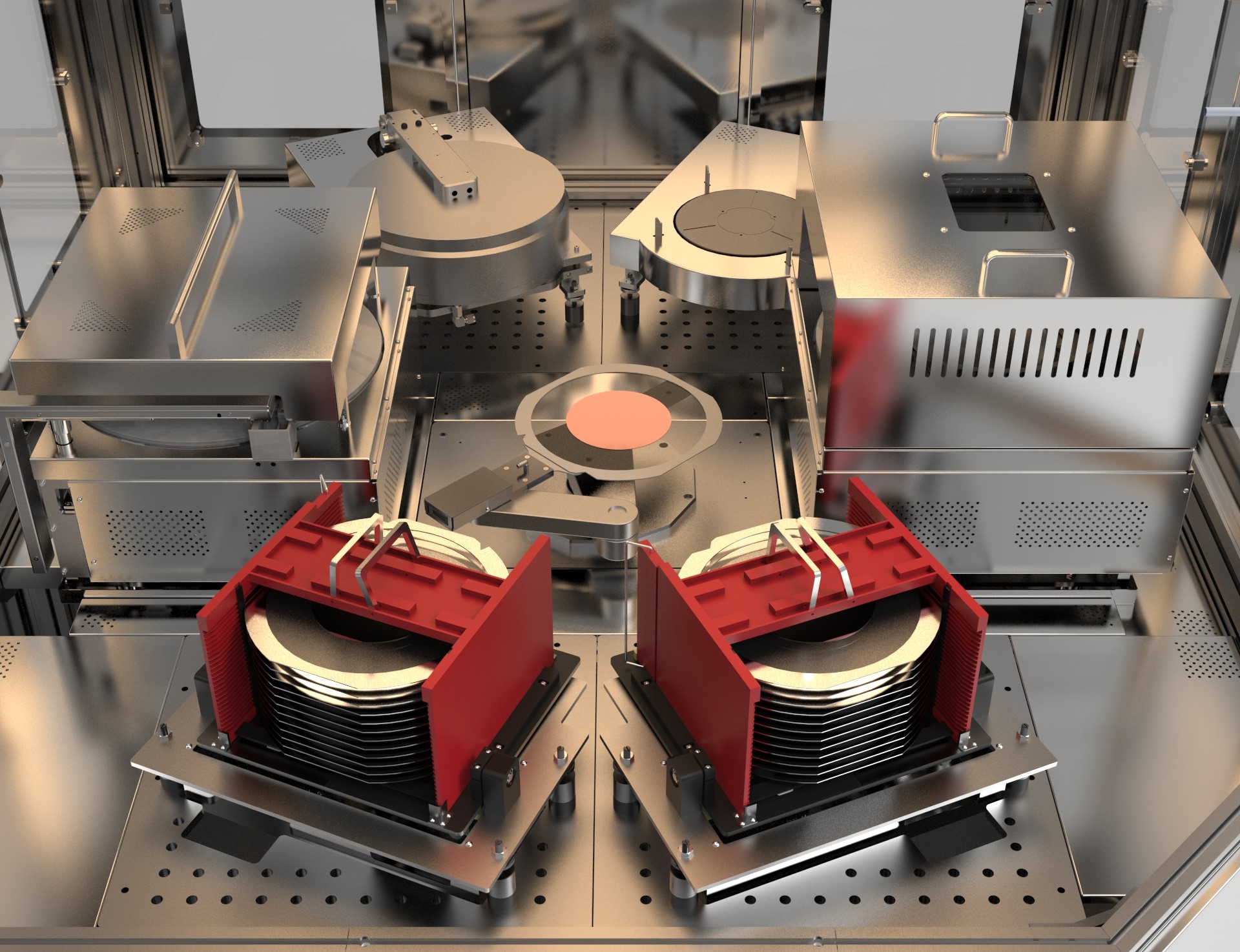
P9000-30 Frame Processing System
- Protective coating before saw or laser scribe
- Wafer and frame cleaning after dicing
- 50mm to 300mm wafers on frames, down to 50 µm thick
- Manual or automatic loading
-

P7000 Wafer Alloy and Anneal System
- Single-wafer metal alloy and anneal up to 500°C
- 50mm to 200mm GaAs, InP and silicon wafers
- Closed chamber with process gases and pump-out
- Up to 23 wafers an hour on one track
-
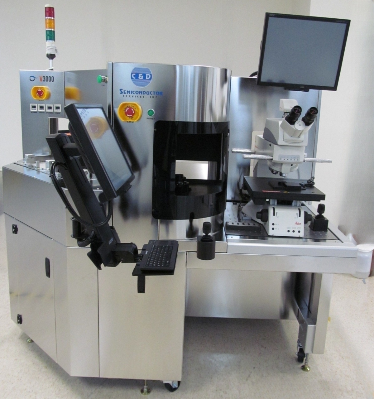
V3000 Macro-Scope Defect Review System
- Macro and microscope defect review on one system
- 50mm to 300mm wafers, dual cassette
- Up to six light sources and a Leica DM8000 microscope
- Defect images and classification stored by wafer ID
-
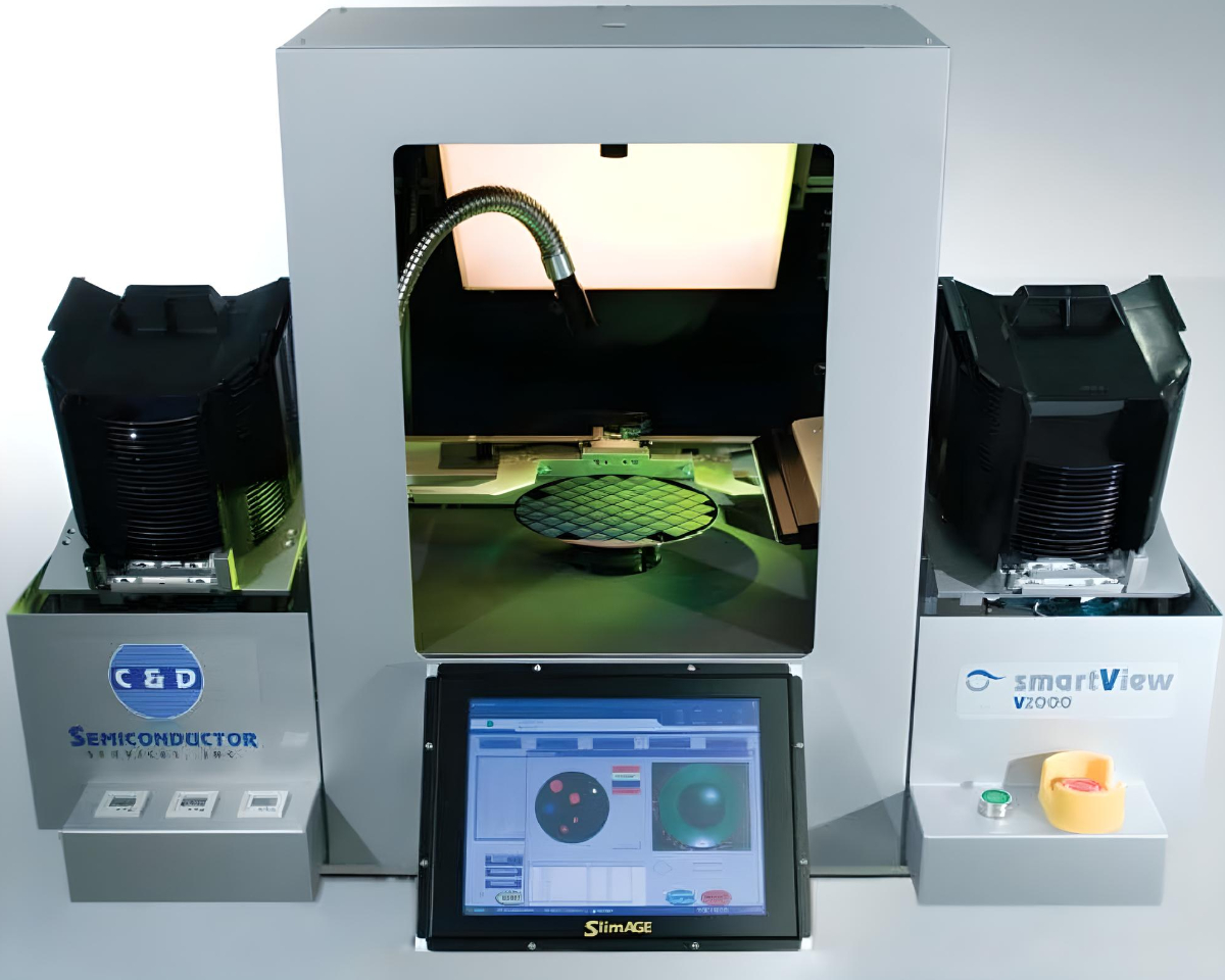
V2000 Bright Light Inspection System
- Bright light macro inspection for 50mm to 200mm wafers
- Up to four light types, each chosen for a defect type
- Auto and manual modes run from engineer recipes
- Tabletop footprint of 45″ x 34″
-
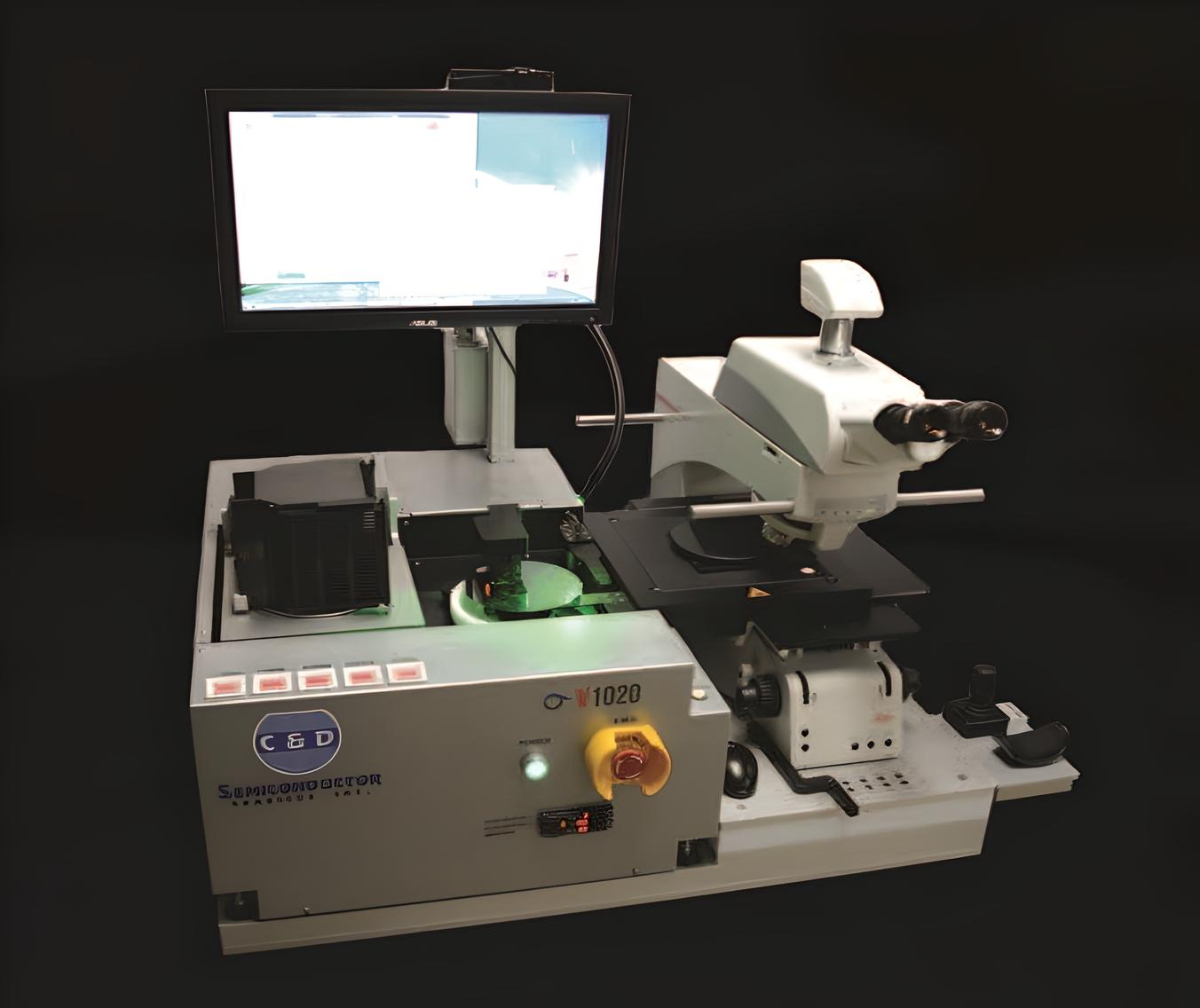
V1020 Microscope Wafer Loader
- Loads wafers from cassette to microscope stage and back
- 50mm to 300mm, with auto detection of two wafer sizes
- More than 200 wafers an hour
- Fits most microscopes