

- Full-size or half-size cabinet for coat, develop and bake modules
- Choice of ducted exhaust, fan filter unit (laminar downflow) or ductless recirculation top
- Installation and training arranged and quoted, delivered by our UK and European after-sales team
- Waste bottle containment with optional drain bottles
- Exhausted drawer for material storage and pressure vessels
- Sash for a clean environment, fume containment and operator safety
- CE marked
Semiconductor Wafer Processing Equipment
Wafer processing equipment covers the tools that pattern and clean a wafer on its way through a fab. That means photoresist coating, developing and baking for lithography, wet cleaning and etching, metal lift-off, temporary bonding for thinning and alloying, along with the heated DI water and chemistry that feed the wet steps. SiSTEM supplies equipment for each of these from four manufacturers, to university cleanrooms and production fabs, and our after-sales team installs and supports what we supply.
Lithography: coat, develop and bake
Photoresist is spun onto the wafer, baked to drive off solvent, exposed, then developed and baked again. Film thickness and bake uniformity decide how well the pattern transfers, so spin speed and plate temperature both have to repeat from one wafer to the next.
For standalone tools, CEE’s Apogee spin coaters, spin developers and bake plates cover research and small-volume production, and the X-Pro II puts them together in one integrated wet bench workstation. They’re very popular with universities and research institutes across the UK and Europe, and with spin-out companies.
For automated coat and develop, C&D Semiconductor builds two platforms. The P9000 cluster tool stacks coater, developer, hot plate, chill plate and vapour prime modules around a central robot, for wafers from 50mm to 300mm. The P8000 linear track runs the same steps in series for 50mm to 200mm wafers, and its smartPro controls can also replace the card cages on existing SVG 8X tracks.
Wet processing and cleaning
Most front-end processes start or finish in liquid. Modutek’s semiconductor wet benches run cleaning, etching, rinsing and drying in one exhausted cabinet, from manual process stations to fully automated lines. Acid and base benches are built in FM4910 polypropylene and solvent benches in stainless steel, and megasonic tanks can be added for particle removal and post-CMP cleaning.
C&D adds two single-wafer processes. Its metal lift-off system strips resist and lifts metal in heated solvent, dry in and dry out, and its wafer scrubber cleans with high-pressure spray and brushes.
Temporary bonding and debonding
Wafers thinned below about 100 µm are bonded to a carrier first, then released once the back-side work is done. CEE’s Apogee Temporary Wafer Bonder takes substrates from 2″ to 300mm, with both platens heated to 300°C and bond force from 550 to 12,000 N. Two debonders release the pair. The Apogee Thermal Slide Debonder slides the carrier off a heated wax or thermoplastic bond, and the Mechanical Debonder peels it away at room temperature. See temporary wafer bonding and debonding for how to choose between them.
Alloy and anneal
C&D’s P7000 is a single-wafer alloy and low-temperature anneal system working up to 500°C in a controlled gas atmosphere. It’s used for ohmic contacts on GaAs, InP, GaN and SiC.
Heated DI water and process chemistry
Wet benches and process tools often need DI water or chemistry at a set temperature. Process Technology’s inline water and chemical heaters are chosen to suit the chemistry and flow rate, and SiSTEM supplies and installs them in the UK and Ireland.
Choosing wafer processing equipment
Most specifications come down to the wafers, the process chemistry and the volume. A research cleanroom running many processes on small wafers usually wants flexible standalone tools, while a production line wants the steps automated and linked. Send us those details and we’ll work through the options with the manufacturer’s engineers.
Wafer processing equipment questions
What is wafer processing equipment?
The tools that coat, develop, bake, clean, etch, bond and anneal wafers during fabrication. On this page that means spin coaters, developers and bake plates, coat and develop tracks, wet benches, lift-off and scrubbing systems, bonders and debonders, alloy systems and process heaters.
What’s the difference between a cluster tool and a linear track?
A cluster tool such as the C&D P9000 arranges its modules round a central robot, so wafers can move between them in any order and several modules work in parallel. A linear track such as the P8000 moves wafers through its modules in series.
Can an existing SVG 8X track be upgraded?
Yes. C&D’s smartPro control system replaces the SVG 8X card cages, and the existing cables plug into it. Operators then use the same Windows interface as a new P8000.
Which wafer sizes do these tools handle?
It depends on the tool. The C&D P9000 takes 50mm to 300mm and the P8000 50mm to 200mm, and CEE’s bonder takes 2″ to 300mm. Each product page gives its own range.
Buying through SiSTEM
We supply and support CEE and Modutek equipment across the UK and Europe, and C&D Semiconductor and Process Technology equipment in the UK and Ireland. If a tool goes down, we stay on the fault with the manufacturer until you confirm it’s working properly again. Get a quote, or contact us with your wafer sizes and process.
Wafer Processing Products
-
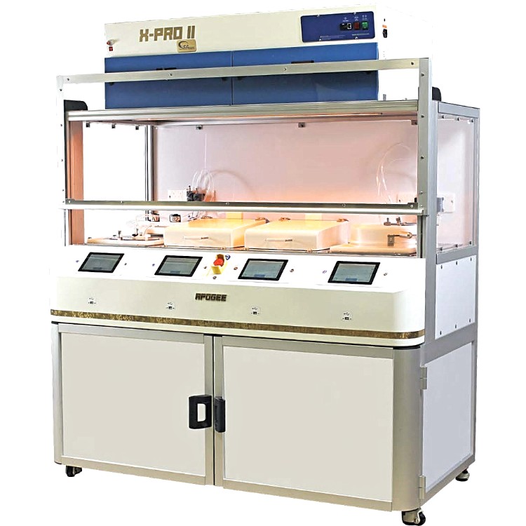
X-Pro II Workstation
-
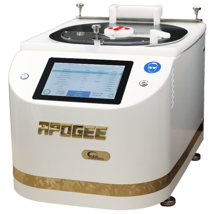
Apogee 200 Spin Coater
- Benchtop spin coater with a compact footprint
- Wafers up to 200 mm round and squares up to 6” x 6”
- Spin speed up to 12,000 rpm, repeatable to 0.2 rpm
- High-density polyethylene (HDPE) spin bowl
- Full-colour 7-inch touchscreen
- Benchtop, flange or deck mounting
- Fits the X-Pro II workstation
-
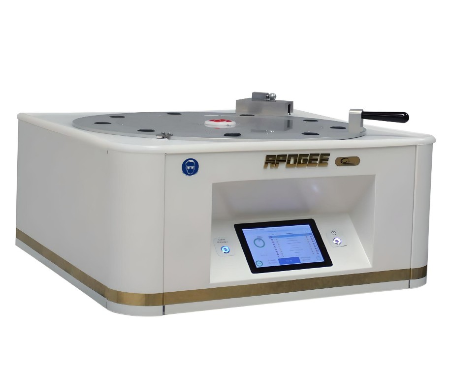
Apogee 450 Spin Coater
- Benchtop spin coater for large substrates
- Wafers up to 450 mm round and squares up to 14” x 14”
- Spin speed up to 6,000 rpm, repeatable to 0.2 rpm
- Indirect drive keeps the motor out of the chemical path
- Full-colour 7-inch touchscreen
- Benchtop, flange or deck mounting
- Fits the X-Pro II workstation
-
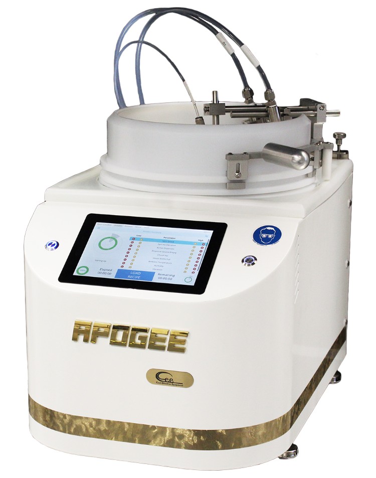
Apogee 200 Spin Developer
- Benchtop spin developer for wafers up to 200 mm and squares up to 6” x 6”
- Spray or stream developer dispense
- Top and backside DI water rinse
- Spin speed up to 12,000 rpm
- Optional nitrogen blow-off
- Fits the X-Pro II workstation
-
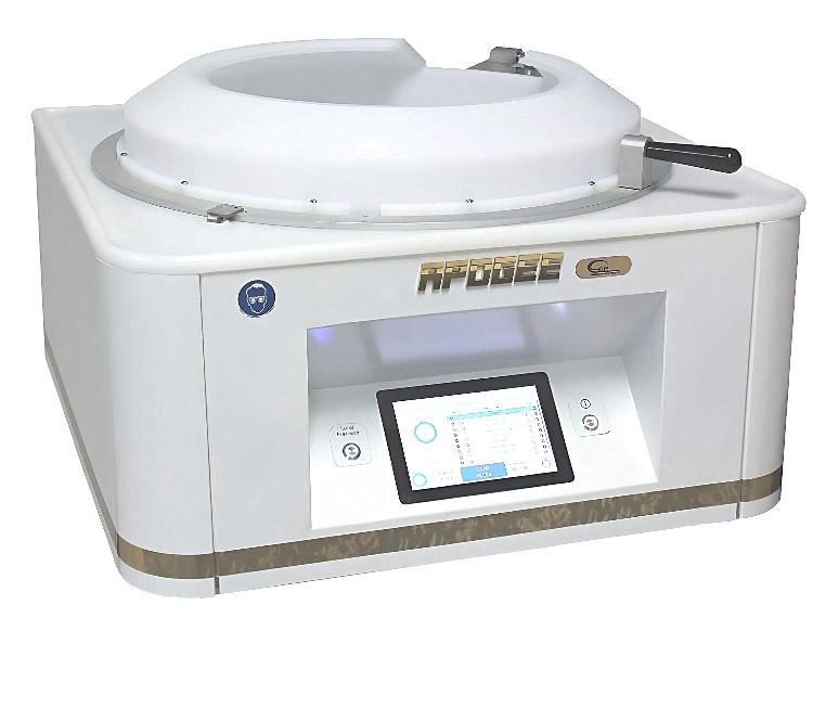
Apogee 450 Spin Developer
- Benchtop spin developer for wafers up to 450 mm and squares up to 14” x 14”
- Fanjet spray, side-angle puddle and stream dispense
- Up to four spray or stream nozzles
- Optional auto-drain separator
- Benchtop, flange or deck mounting
- Fits the X-Pro II workstation
-
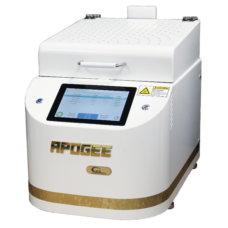
Apogee 200 Bake Plate
- Benchtop bake plate for wafers up to 200 mm and squares up to 8” x 8”
- Ambient to 300°C, or 400°C as an option
- ±0.3% uniformity across the working surface
- Contact, vacuum or proximity baking
- Smart Pins set the proximity height under program control
- Cool-touch exhausted stainless steel hood
- Benchtop or flange mounting; fits the X-Pro II workstation
-
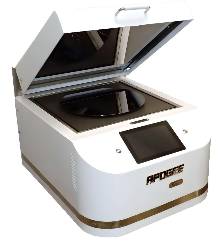
Apogee 300 Bake Plate
- Bake plate for wafers up to 300 mm and squares up to 12”
- Ambient to 300°C, or 400°C as an option
- ±0.3% uniformity across the working surface
- Contact, vacuum or proximity baking
- Smart Pins set the proximity height under program control
- Cool-touch exhausted stainless steel hood
- Benchtop, flange or deck mounting; fits the X-Pro II workstation
-
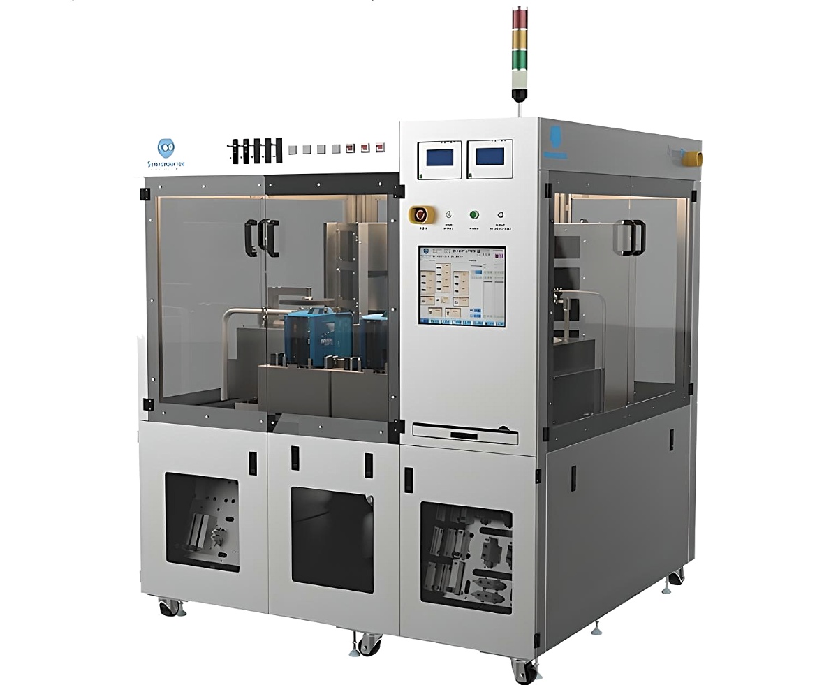
P9000 Coat and Develop Cluster Tool
- Coat, develop, bake, prime and chill modules in any mix
- 50mm to 300mm wafers, up to three sizes without hardware change
- Spray coating, metal lift-off, alloy and optical EBR options
- Built in San Jose, supplied and supported by SiSTEM
-
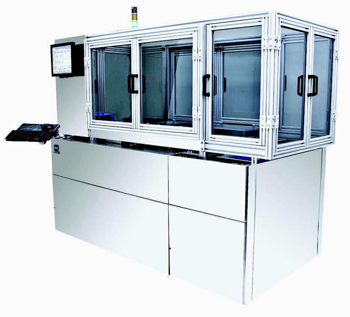
P8000 Linear Coat and Develop Track
- Linear coat and develop track for 50mm to 200mm wafers
- Coater, developer, hot plate, chill, vapour prime and scrubber modules
- Built new, with obsolete parts designed out
- Built in San Jose, supplied and supported by SiSTEM
-
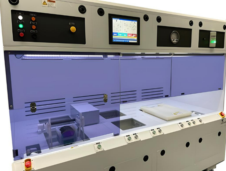
Custom Wet Benches and Wet Process Stations
- Manual, semi-automated or fully automated
- FM4910 for acids and bases, stainless steel for solvents
- Built and tested in San Jose, California
- Installed and serviced by SiSTEM in the UK and Europe
-
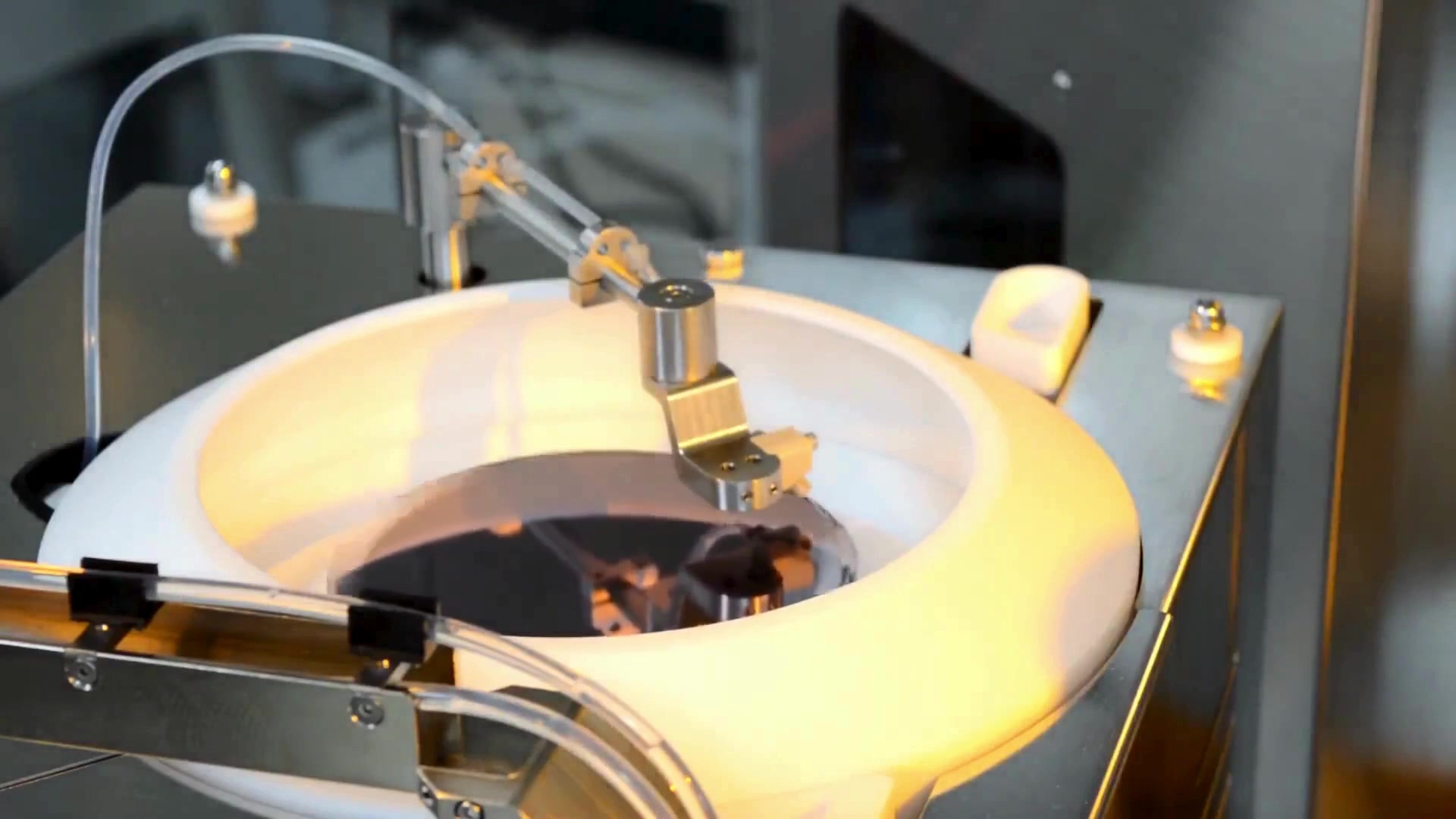
Metal Lift-Off System
- Solvent soak and high-pressure spray lift-off in one module
- Dry-in, dry-out, cassette to cassette
- Heated acetone, IPA, NMP and other solvents
- Separate drains for metal recovery
-
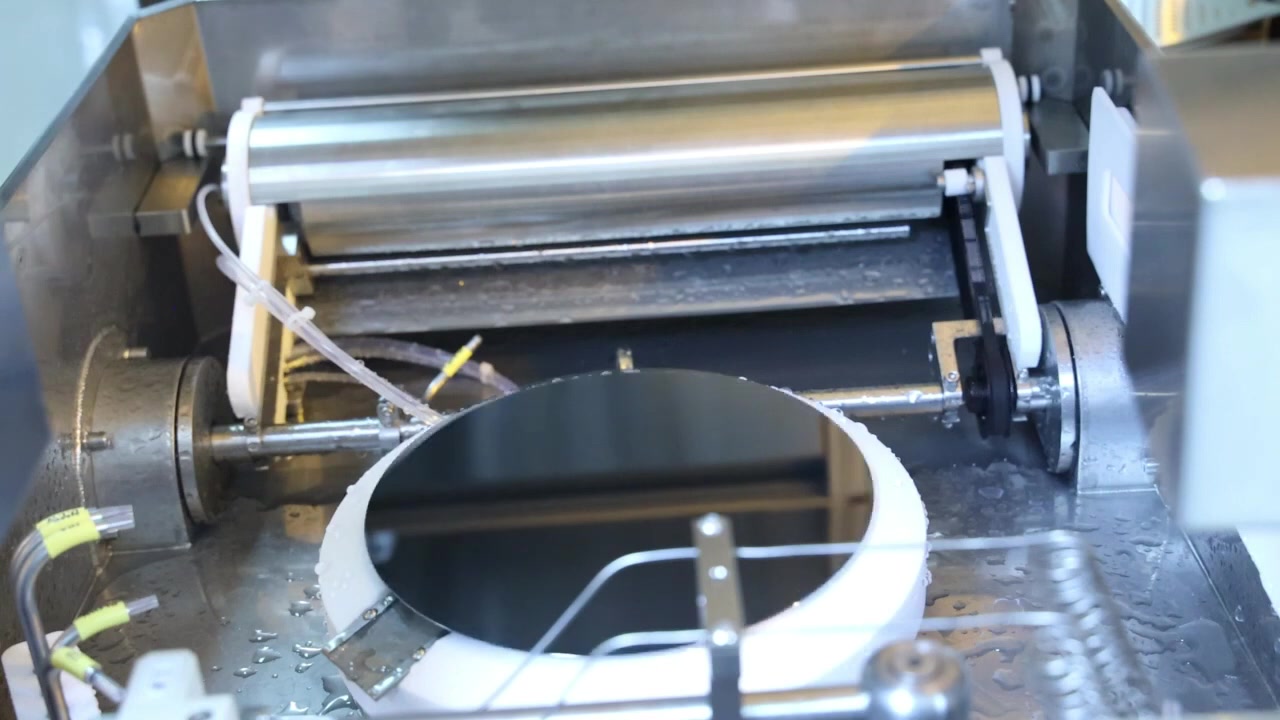
Wafer Scrubber and Cleaning System
- Roller brush and high-pressure spray cleaning
- Wafers, grinding carriers and mask blanks
- 100mm to 300mm, one to four scrubber modules
- Dry-in, dry-out, with two chemistries
-
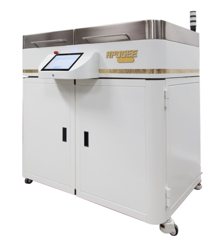
Apogee Temporary Wafer Bonder
- Vacuum bonding of device wafers to carrier substrates
- Substrates from 2” to 300 mm
- Two heated platens, independently controlled to 300°C
- Bond force 550 to 12,000 N
- Wafers held apart until the chamber is evacuated, keeping voids out of the bond line
- DataStream logs every bond cycle
- CE marked
-
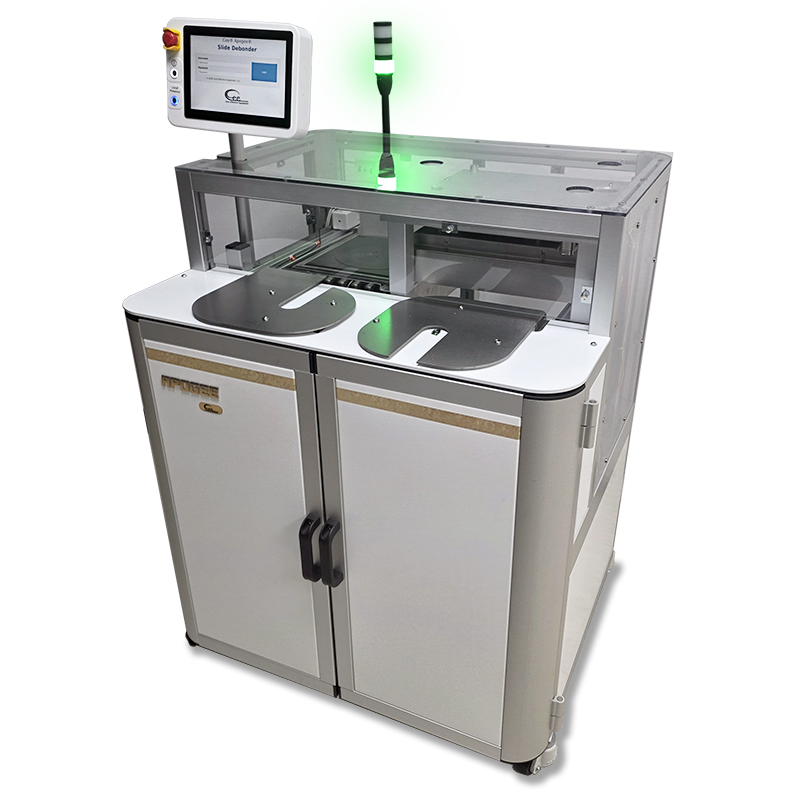
Apogee Thermal Slide Debonder
- Semi-automated thermal slide debonder for wax and thermoplastic adhesives
- Substrates from 2” to 200 mm
- Two heated platens, independently controlled to 300°C
- Recipe-controlled slide force (1 to 100 N) and speed
- DataStream logs force and cycle time for every wafer
- Replaces CEE’s earlier 1300CSX slide debonder
- CE marked
-
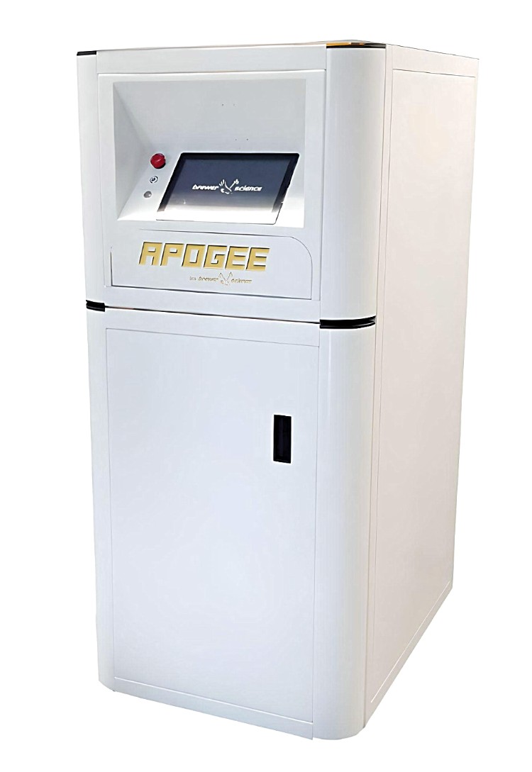
Mechanical Wafer Debonder
- Room-temperature peel debonding of temporarily bonded wafer pairs
- Substrates from 50 mm to 200 mm, device wafer on film frame
- Peel force 1 to 75 N, set by recipe
- Up to 20 wafers an hour
- Excess force sensing stops the peel automatically
- DataStream logs force and cycle time for every wafer
- CE marked
-

P7000 Wafer Alloy and Anneal System
- Single-wafer metal alloy and anneal up to 500°C
- 50mm to 200mm GaAs, InP and silicon wafers
- Closed chamber with process gases and pump-out
- Up to 23 wafers an hour on one track
-
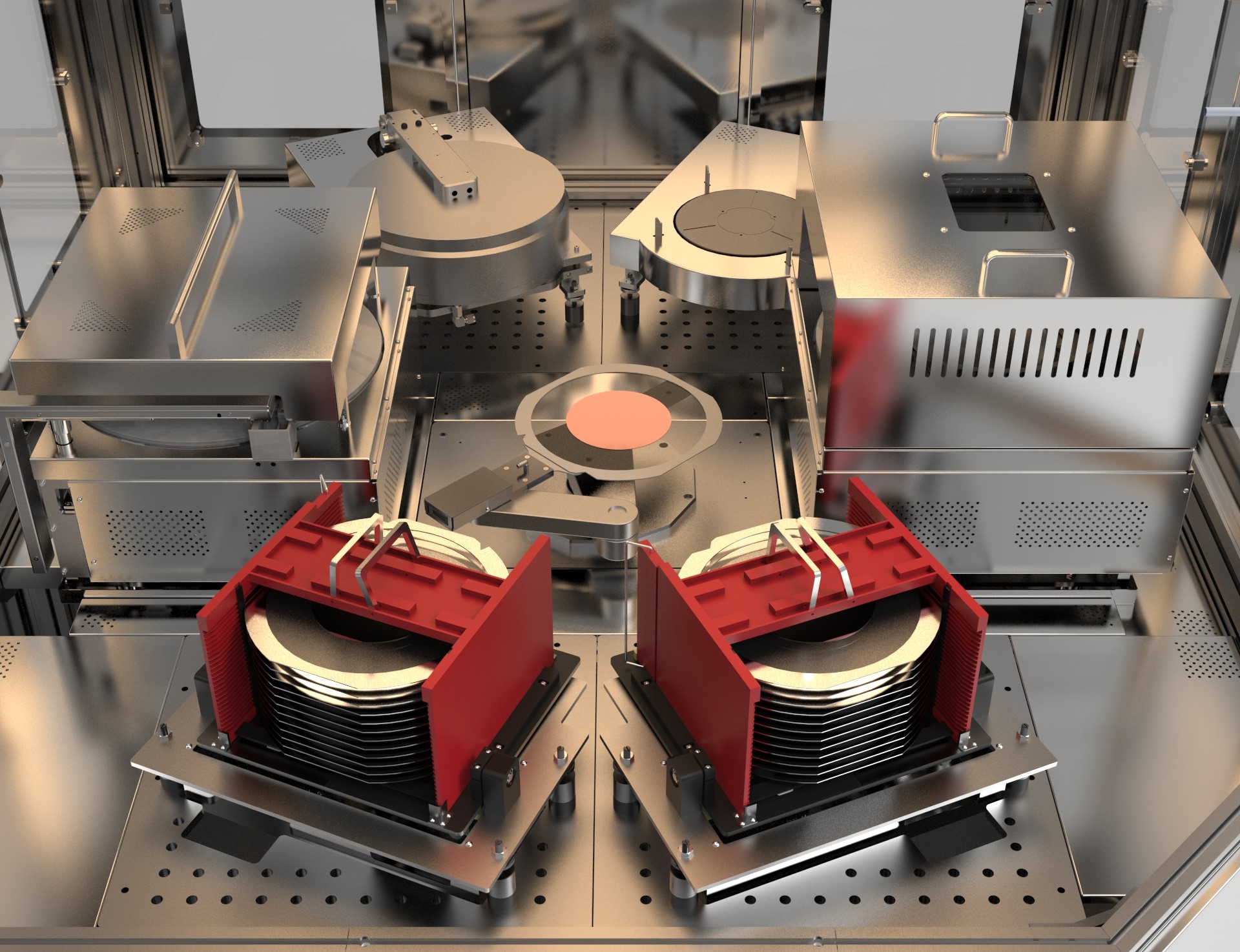
P9000-30 Frame Processing System
- Protective coating before saw or laser scribe
- Wafer and frame cleaning after dicing
- 50mm to 300mm wafers on frames, down to 50 µm thick
- Manual or automatic loading