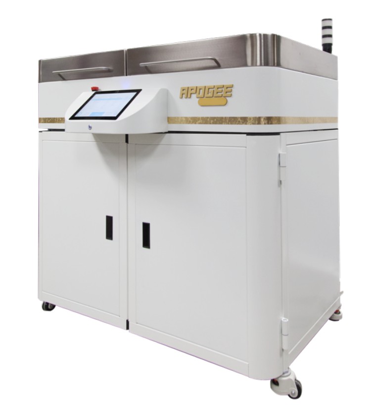
Apogee Temporary Wafer Bonder
Cost Effective Equipment Apogee Wafer Bonder
The Cost Effective Equipment Apogee Temporary Wafer Bonder is a state-of-the-art bonding solution designed to accelerate product development and reduce production costs during semiconductor wafer processing. Engineered for high yield and throughput, the Apogee Bonding System delivers unparalleled performance without the complexities and expenses associated with full automation.
Wafer Bonder Key Benefits and Features
Versatile Substrate Compatibility
The Apogee Wafer Bonder supports a wide range of substrate sizes from 50 mm to 300 mm, accommodating diverse semiconductor materials and device configurations. This flexibility ensures that the system meets the needs of various semiconductor fabrication processes.
Advanced Thermal Management
Equipped with dual heated platens featuring independent temperature controls, the Cost Effective Equipment Apogee Wafer Bonder minimises thermal defects and ensures uniform heat distribution. Self-leveling platens further reduce total thickness variation, enhancing bonding quality and consistency.
Void-Free Bonding Process
An evacuated bond chamber, combined with a unique pre-bond evacuation step where the carrier and device are kept separate, effectively eliminates voids. This critical feature ensures a flawless bond interface, significantly improving device reliability.
DataStream™ Technology Integration
Leveraging DataStream™ technology, the Apogee Temporary Wafer Bonder offers advanced process monitoring and control capabilities. With push notifications sent to any web-enabled device, engineers can stay informed about the bonding process in real-time, ensuring optimal operation and efficiency.
Unmatched Programmability and Connectivity
Intuitive Touch Screen Interface
The user-friendly touch screen interface provides easy access to a virtually unlimited number of user-defined recipe program steps. With 0.1-second resolution for step times and detailed process traceability, the Cost Effective Equipment Apogee Wafer Bonder enables precise control over every aspect of the bonding process.
Comprehensive Process Monitoring
On-line graphical process charts and logs display real-time data on piston pressure, force, temperature, vacuum, and cycle time. This level of detail supports advanced process optimisation and troubleshooting, ensuring consistent bonding performance.
Seamless Data Management
The system’s connectivity options, including USB and Ethernet ports, facilitate the effortless uploading and downloading of process parameters. Coupled with DataStream™ technology, this feature enables seamless data management and analysis for continuous process improvement.
Proven Reliability and Throughput
High Throughput with Exceptional Yield
Achieving an estimated throughput of 14-20 wafers per hour (WPH), the Apogee Wafer Bonder is optimised for process-dependent performance. This efficiency, paired with a broad compatibility with wafer materials like SiC, GaN, GaAs, InP, sapphire, silicon, and glass, ensures high yields across a wide spectrum of semiconductor applications.
Outstanding System Uptime & Serviceability
With system uptime exceeding 99% over a 12-month period and a mean time to repair (MTTR) of less than 24 hours, the Apogee Wafer Bonder stands as a beacon of reliability in semiconductor wafer bonding technology. Furthermore, its impressive mean time between failures (MTBF) of more than 600 hours and 6,000 cycles underscores the system’s durability and long-term performance.
The Cost Effective Equipment Apogee Wafer Bonder represents a significant leap forward in semiconductor wafer bonding technology. By combining flexible substrate handling, advanced thermal management, and cutting-edge programmability with unparalleled system reliability, the Apogee Wafer Bonder is set to redefine the standards of semiconductor production.
Contact us today to discuss your project in more detail and see how Cost Effective Equipment Apogee Temporary Wafer Bonder will help you innovate your wafer processing. Alternatively, get a quote quickly now.