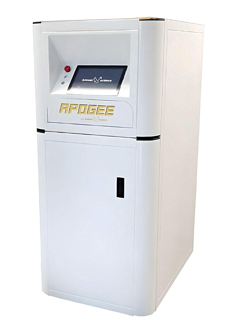
Mechanical Wafer Debonder
Cost Effective Equipment Apogee Mechanical Wafer Debonder
The cutting-edge Cost Effective Equipment Apogee Mechanical Wafer Debonder is a revolutionary tool designed to seamlessly integrate into both research and development environments and small volume production lines where semiconductor wafer processing takes place. This state-of-the-art mechanical wafer debonder is tailored for operations demanding the use of high-temperature bonding materials, coupled with the necessity for low-stress, room-temperature debonding.
The Cost Effective Equipment Apogee Mechanical Wafer Debonder stands as the epitome of innovation in debonding technology, offering unparalleled versatility to meet a wide range of device requirements. Whether your application involves devices with a low thermal budget or necessitates bonding adhesives capable of withstanding high temperatures during post-bond processing, the Apogee Mechanical Debonder emerges as the optimal solution.
Advantages of the Apogee Mechanical Debonder
Minimised Stress
Ensures the integrity of the device wafer by applying precisely controlled forces, minimising stress during the debonding process.
High Throughput
Achieves up to 20 wafers per hour, optimising productivity without compromising quality.
Room Temperature Operation
Allows the use of high-temperature adhesives for post-bond processing, expanding the range of applications.
Clean and Efficient
Eliminates the need for messy solvents typical of solvent wafer debond processes, maintaining a clean operating environment.
Secure Wafer Handling
The device wafer remains securely attached to the film frame throughout the process, significantly reducing the risk of handling damage and device loss.
Wafer Debonder Tool Features & Specs
Substrate Compatibility
Accommodates round substrate sizes from 50 mm to 300 mm, catering to a diverse range of wafer dimensions.
Precision Force Application
Offers a force range of 0 to 100 N (1 to 22 lb), ensuring low stress to the device wafer with failsafe error recovery through excess force sensing.
Compact and Ergonomic Design
The mechanical wafer debonder’s minimised footprint allows for flexible installation in any lab or production setting.
Advanced Programmability
Features a full-color, 7-inch touchscreen display and an intuitive graphical user interface, supporting an unlimited number of user-defined recipe program steps with a 0.1-second resolution for step times.
Streamlined Operation with DataStream™ Technology
Equipped with DataStream™ technology, the Apogee Mechanical Wafer Debonder offers real-time network access for remote monitoring and logging of all critical debonding parameters. This feature enhances process traceability for every wafer, with online graphical process charts and logs available for in-depth analysis.
Ensuring High Yield & Operational Reliability
The Apogee Mechanical Wafer Debonder not only prioritises the performance and reliability akin to track systems but does so without the associated hassle, footprint, and cost. It boasts an impressive operational yield of over 98% and system uptime, affirming its status as a reliable tool for today’s semiconductor fabrication challenges.
The Cost Effective Equipment Apogee Mechanical Wafer Debonder represents a significant leap forward in debonding technology, offering semiconductor manufacturers a versatile, high-throughput, and low-stress solution for the debonding of fully processed thinned device wafers. Its compact design, combined with the advanced capabilities of DataStream™ technology and comprehensive programmability, makes it an invaluable asset for accelerating product development and enhancing production efficiency.
Get a quote today to see how the Cost Effective Equipment Apogee Mechanical Wafer Debonder will lift your semiconductor wafer processing to new heights of excellence. Trust in CEE’s proven track record and experience the difference that performance-driven technology can make in your operations. Alternatively, contact us if you have any questions before requesting a quote to discover how this state-of-the-art equipment can revolutionise your wafer processing and help you achieve exceptional outcomes.