- Versatile Substrate Compatibility
- Advanced Thermal Management
- Void-Free Bonding Process
- High Throughput with Exceptional Yield
- Outstanding System Uptime & Serviceability
- Comprehensive Process Monitoring
Email: info@sistemtechnology.com Call: +44 (0)1327 362 844
Temporary Wafer Bond & Debond Tools
Temporary wafer bonding and debonding for advanced semiconductor processing
Temporary wafer bonding and debonding tools enable thin, fragile and high-value substrates to be safely supported throughout demanding semiconductor processes such as wafer thinning, backgrinding, TSV formation, metallisation, compound semiconductor processing and advanced packaging.
SiSTEM Technology supplies CEE® Apogee® wafer bonding and debonding systems for laboratories, pilot lines and production environments where process repeatability, substrate protection and yield are critical. These tools support the controlled bonding of device wafers to carrier substrates, allowing the bonded wafer pair to undergo downstream processing before being carefully debonded, cleaned, inspected and prepared for the next stage of manufacture.
Temporary wafer bonding is vital for the production of 3D integrated circuits (ICs), power devices and Fan-Out Wafer Level Packaging (FoWLP) wafers, as well as for the handling of delicate substrates such as compound semiconductors, thin silicon, glass, sapphire and other advanced materials.
What is temporary wafer bonding?
Temporary wafer bonding is the process of bonding a device wafer to a carrier wafer so that thin or delicate substrates can be safely handled during demanding manufacturing steps. This is particularly important where the device wafer is too fragile to process unsupported, or where downstream processes require controlled support, flatness and mechanical stability.
In a typical process, an adhesive is applied to the wafer, the device wafer is aligned with a suitable carrier, and the bonded pair is processed under controlled temperature, pressure and vacuum conditions. Once bonded, the wafer pair can be thinned, polished, etched, metallised or otherwise processed before the carrier is removed through a suitable debonding method.
The Cost Effective Equipment Apogee® Temporary Wafer Bonder provides controlled adhesive bonding for a wide range of semiconductor and advanced substrate applications, helping users manage key process variables such as flatness, alignment, void reduction, temperature consistency, bonding force and carrier compatibility.
Temporary wafer bonding and debonding workflow
A successful temporary wafer bond and debond process depends on each stage of the workflow being controlled and compatible with the materials, wafer sizes and downstream processes involved.
– Adhesive selection and coating
– Device wafer and carrier wafer preparation
– Temporary wafer bonding under controlled temperature, vacuum and force
– Wafer thinning, grinding, polishing or downstream processing
– Thermal, mechanical or chemical debonding, depending on the adhesive system
– Cleaning, inspection, dicing, packaging or further processing
By selecting the correct bonding and debonding route at the start of process development, manufacturers can reduce substrate damage, improve process repeatability and support higher-yield handling of thin or high-value wafers.
The essence of wafer bonding
With the semiconductor industry’s shift towards smaller, more powerful and more highly integrated devices, the demand for advanced wafer bonding solutions has increased significantly. Temporary substrate bonding is especially important for substrates thinner than 100µm, where unsupported handling can lead to breakage, bowing, cracking or contamination.
The Cost Effective Equipment Apogee® Temporary Wafer Bonding and Debonding tools help mitigate these risks by supporting precise downstream processing such as through-silicon vias (TSV), metal plating, thinning, etching, polishing and advanced packaging. Following these processes, the bonded pair is debonded, cleaned, diced and packaged, ready for integration into final devices or further manufacturing steps.
Optimised bonding conditions
Following the adhesive material specifications, the CEE® Apogee® Temporary Wafer Bonder uses heated platens to bring the adhesive to the correct process temperature, helping it reach its optimal state for strong, uniform bonding. The device wafer is precisely aligned and centred on the lower platen before being bonded to the carrier wafer, with mechanical fixtures supporting alignment without direct contact during loading.
Vacuum-sealed bonding chamber
Once aligned, the bonding chamber is sealed and vacuum is applied to remove air from the process environment. Programmable piston force then helps ensure uniform adhesive spread and full wafer coverage. After bonding, the wafer pair is cooled on a dedicated plate, solidifying the adhesive and preparing the bonded assembly for subsequent processing.
Critical parameters for high-quality wafer bonding
The quality of wafer bonding is influenced by several critical parameters. These become even more important as semiconductor devices move towards finer features, thinner substrates, advanced packaging formats and more complex material stacks.
Flatness and TTV
Total Thickness Variation (TTV) and flatness are essential for uniform bonding. Poor flatness can contribute to voids, stress points and uneven support, increasing the risk of defects or substrate damage during downstream processing.
Alignment
Accurate wafer-to-carrier alignment is critical for consistent bonding and downstream process accuracy. This is particularly important where feature placement, lithography, etching or metallisation steps depend on reliable wafer positioning.
Void reduction
Voids can weaken the bonded structure, reduce process uniformity and increase the risk of delamination or breakage. Controlled vacuum, adhesive flow and bonding force help reduce trapped air and improve bond quality.
Temperature control
Uniform temperature control helps ensure consistent adhesive behaviour across the wafer surface. This supports reliable adhesive flow, curing or softening, depending on the chosen bonding material.
CTE compatibility
The coefficient of thermal expansion (CTE) of the wafer, carrier and adhesive materials must be considered carefully. Poor compatibility can create stress during heating, cooling or downstream thermal processes, potentially leading to cracking or delamination.
Bonding force
The correct bonding force helps create a strong, uniform bond without damaging fragile substrates. Programmable force control allows users to optimise process conditions for different wafer sizes, materials and adhesive systems.
Temporary wafer debonding
Once downstream processing is complete, the bonded wafer assembly must be carefully debonded so the device wafer can continue to inspection, cleaning, dicing, packaging or integration. The correct debonding method depends on the adhesive material, wafer size, substrate type, device sensitivity and overall process requirements.
For wax and thermoplastic adhesive processes, the CEE® Apogee® Thermal Slide Debonder provides a controlled, semi-automated approach to wafer separation. Using dual heated platens, vacuum control and programmable slide force, speed, temperature and timing, it helps reduce manual handling risk while improving repeatability and process traceability.
For selected applications, the CEE® Apogee® Mechanical Wafer Debonder may also be suitable, depending on the bonding material used and the specific requirements of the wafer stack.
Once the device wafer has been debonded from the carrier wafer, it can be sent for further processing, inspection, cleaning, dicing, packaging or integration into final products.
CEE® temporary wafer bonding and debonding tools
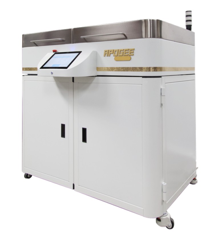
Apogee® Temporary Wafer Bonder
The CEE® Apogee® Temporary Wafer Bonder provides controlled adhesive bonding of device wafers to carrier substrates, supporting downstream processes such as thinning, grinding, polishing, etching, metallisation and advanced packaging. Designed for precision and repeatability, it helps users optimise key process conditions such as temperature, pressure, vacuum and alignment.
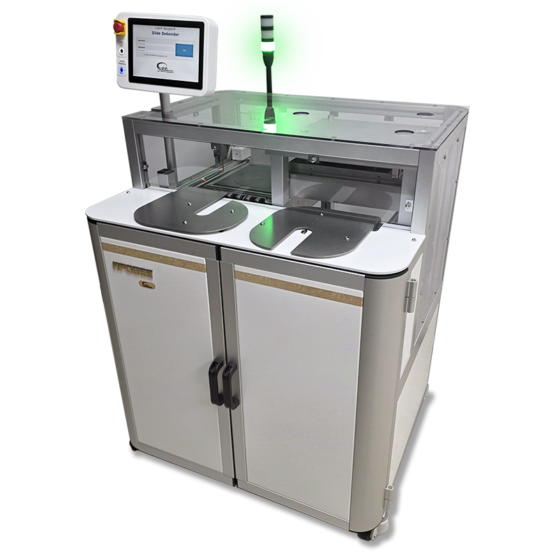
Apogee® Thermal Slide Debonder
The CEE® Apogee® Thermal Slide Debonder provides semi-automated thermal slide debonding for wax and thermoplastic adhesive processes. With dual heated platens, programmable force and speed control, recipe-based operation and DataStream™ process logging, it offers a controlled route to repeatable wafer separation for substrates from 2 inch to 200 mm.
The system is designed to reduce the risks associated with manual debonding, including substrate breakage, operator-dependent variation and inconsistent separation. It is suitable for R&D, pilot production and production environments where gentle handling, repeatability and traceability are essential.
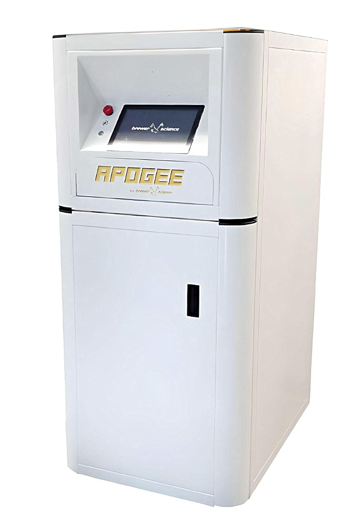
Mechanical Wafer Debonder
The CEE® Mechanical Wafer Debonder provides an alternative debonding route for selected temporary bonding processes where mechanical carrier release is appropriate for the bonding material, wafer stack and substrate handling requirements.
Choosing the right temporary wafer debonding method
The correct debonding route depends on the adhesive material, wafer size, substrate type, device sensitivity, downstream process history and required throughput. Thermal slide debonding is particularly useful where waxes or thermoplastic adhesives are used and where controlled heat, vacuum and programmed slide force can help reduce handling risk.
– Thermal slide debonding is suited to wax and thermoplastic adhesive systems where heat-assisted separation is required.
– Mechanical debonding may be suitable for selected bonding stacks where controlled mechanical release is appropriate.
– Chemical debonding may be used where the bonding material requires solvent or chemical release.
– Application-specific evaluation is recommended for fragile substrates, compound semiconductors, thin wafers and advanced packaging applications.
SiSTEM Technology can help you discuss your process requirements with CEE and identify which temporary bonding and debonding route is most appropriate for your application.
Why temporary wafer bonding and debonding?
Enabling thinner wafers
As semiconductor devices shrink and functionality increases, the need for thinner wafers becomes more important. Temporary bonding tools allow wafers to be supported while being thinned beyond what would otherwise be practical, helping enable ultra-thin devices, flexible electronics, advanced packaging and compound semiconductor applications.
Complex device fabrication
Advanced semiconductor devices, including 3D stacked integrated circuits, MEMS, sensors and power devices, often require multiple layers of fabrication and careful handling through several processing stages. Temporary bonding and debonding tools provide a controlled way to support these structures before final assembly.
Enhanced process flexibility
Temporary bonding and debonding technologies offer valuable process flexibility, accommodating a wide range of materials, adhesives, carrier substrates and downstream processing conditions. This adaptability is crucial in a sector where innovation, material diversity and device complexity continue to develop rapidly.
Benefits of temporary bonding and debonding tools
Increased yield and reliability
By enabling the handling of wafers and devices through challenging processing steps without damage, temporary bonding and debonding tools can help improve yield and reliability. Controlled bonding and debonding reduce the risk of breakage, delamination and process-related defects.
Cost efficiency
The ability to process thinner wafers and more complex devices without unnecessary loss or damage helps reduce material waste and improve fabrication efficiency. This is especially important when working with high-value substrates such as SiC, GaN, GaAs, InP, sapphire, silicon and glass.
Process repeatability
Recipe-controlled bonding and debonding tools help users define, store and repeat critical process parameters. This is valuable in both R&D and production environments where repeatability, traceability and process control are essential.
Support for innovation
Temporary bonding and debonding technologies are important enablers for next-generation semiconductor devices. By supporting thin wafer handling, advanced material processing and complex device structures, these tools help researchers and manufacturers develop new processes with greater confidence.
Industries and applications
Semiconductor manufacturing
Temporary wafer bonding and debonding tools are used in semiconductor manufacturing for wafer backgrinding, thinning, polishing, etching, metallisation, layer stacking and other advanced wafer processing steps.
MEMS and sensors
In MEMS and sensor production, temporary bonding and debonding tools enable the precise handling and processing of delicate structures, helping support device functionality and reliability in automotive, medical, industrial and consumer electronics applications.
Advanced packaging
Temporary bonding and debonding play a key role in advanced packaging techniques such as 3D IC integration, wafer-level packaging and fan-out wafer-level packaging, where multiple semiconductor devices or layers may be integrated into a single package for enhanced performance and functionality.
Compound semiconductors
Compound semiconductor substrates such as SiC, GaN, GaAs and InP can be fragile, high-value and challenging to process. Temporary bonding and controlled debonding can help support these substrates during thinning, polishing and downstream device processing.
Flexible and wearable electronics
The support provided by temporary wafer bonding and debonding technologies is valuable in the development of flexible and wearable electronics, where thin, lightweight and mechanically sensitive materials may need to be processed safely and consistently.
Temporary wafer bonding and debonding FAQs
What is temporary wafer bonding?
Temporary wafer bonding is the process of bonding a device wafer to a carrier wafer so that thin, fragile or high-value substrates can be safely handled during downstream processing.
Why is temporary wafer debonding important?
Temporary wafer debonding releases the processed device wafer from the carrier once thinning, grinding, etching, metallisation or other process steps have been completed. A controlled debond process helps reduce the risk of wafer damage, breakage or contamination.
What is thermal slide debonding?
Thermal slide debonding uses controlled heat and slide force to separate a bonded wafer pair. It is often used with wax and thermoplastic adhesive systems where a controlled, repeatable and lower-risk separation process is required.
Which wafer materials can be used in temporary bond and debond processes?
Temporary bonding and debonding processes may be used with silicon, glass, sapphire and compound semiconductor materials such as SiC, GaN, GaAs and InP, depending on the tool configuration, bonding material and process requirements.
Which CEE® tool is suitable for thermal debonding?
The CEE® Apogee® Thermal Slide Debonder is the current thermal slide debonding solution for wax and thermoplastic adhesive processes. It supports substrates from 2 inch to 200 mm and provides recipe-controlled temperature, force, speed and timing for repeatable wafer separation.
How do I choose between thermal, mechanical and chemical debonding?
The most suitable debonding method depends on the adhesive material, substrate type, wafer size, device sensitivity and downstream process history. SiSTEM Technology can help you review your process requirements and discuss the most appropriate CEE® tool for your application.
Discuss your temporary wafer bond and debond application
Whether you are developing a new temporary bonding process, improving substrate handling, introducing wafer thinning, or reviewing debonding options for fragile or high-value wafers, SiSTEM Technology can help you identify the right CEE® tool for your application.
Contact SiSTEM Technology to discuss your process requirements, or request a quote for CEE® temporary wafer bonding and debonding tools.
Temporary Bond & Debond Products
-
Apogee Temporary Wafer Bonder
-
Apogee Thermal Debonder
- Semi-automated thermal slide debonder for controlled wafer separation
- Designed for wax and thermoplastic adhesive debonding processes
- Supports substrate sizes from 2 inch to 200 mm
- Dual heated platens with independent temperature control up to 300°C
- Recipe-controlled force, speed, temperature and timing for repeatable processing
- DataStream™ technology for process logging, traceability and remote process management
- Suitable for R&D, pilot production and semiconductor manufacturing environments
-
Mechanical Wafer Debonder
- Minimised Stress
- High Throughput
- Room Temperature Operation
- Secure Wafer Handling
- Clean and Efficient
- Precision Force Application