1300CSX Thermal Slide Debonder
Thermal Slide Wafer Debonder
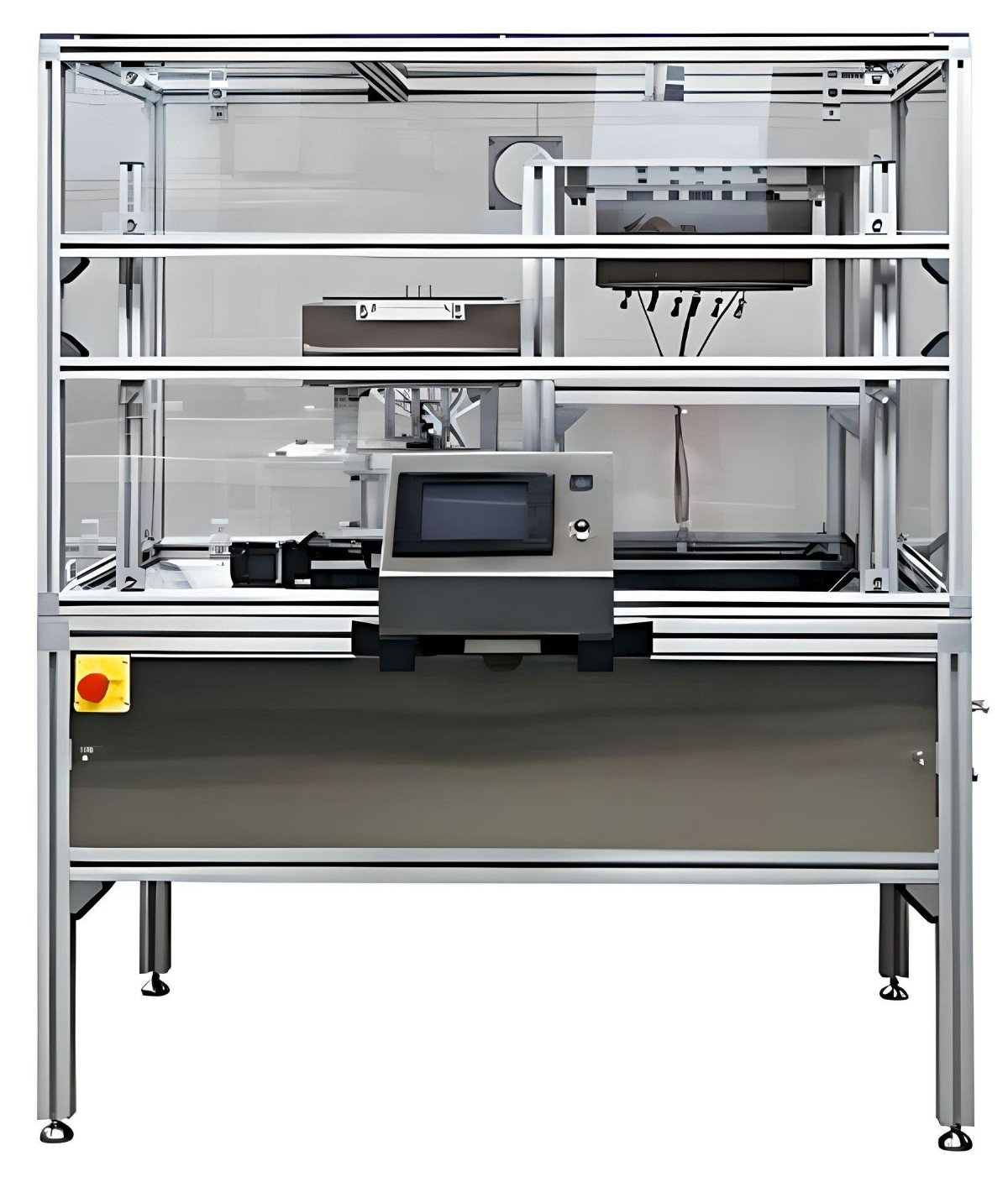
In the rapidly evolving world of semiconductor wafer processing technology, the Cost Effective Equipment 1300CSX Thermal Slide Debonder stands out as a groundbreaking solution, designed specifically for the high-temperature slide-off debonding of thinned compound semiconductor materials. Ideal for materials like GaAs, GaN, InP, and SiC, this Debonder is perfectly suited for laboratory settings, offering engineers the capability to finalise the processing of thinned full wafers within a developmental context.
The 1300CSX Thermal Slide Debonder is not just a tool; it’s an innovation accelerator, enabling internal small-scale prototyping that can significantly speed up product development cycles. This is especially critical in the fast-paced sectors of high-power RF, LED, and solar applications, where time to market can determine the success of new compound semiconductor applications.
Cost Effective Equipment is renowned as a leading supplier of thin-wafer handling technology, and the 1300CSX Debonder is a testament to this reputation. Demonstrating industry-leading precision and performance, this platform is engineered to handle the delicate nature of fully processed, ultrathin device wafers, ensuring their integrity from start to finish.
Key Debonder Benefits
In-House Debonding Capability
Empowers teams to debond fully processed, proprietary ultrathin device wafers within the confines of their own laboratory, ensuring confidentiality and security.
Advanced Data Logging
Offers detailed process feedback and record-keeping, essential for refining processes and ensuring repeatability.
PC Control with Extensive Log Storage
Facilitates virtually unlimited storage for process logs, enhancing traceability and process optimisation.
Compact Design
Ensures easy integration into any laboratory setup without compromising on space.
Tool Features
Network Connectivity
Equipped with RJ-45 Ethernet and USB ports for easy integration into existing networks.
Unrivalled Precision
Bond line axis precision of ±1.5 nm, setting a new standard for debonder accuracy.
Specialised Handling
Features specialised insertion and extraction end effectors with vacuum function, controlled via foot pedal for ease of operation.
Safety and Operation
Enhanced with a visual and audible light tree alarm, light curtain operation, and continuous abort override for super users.
Accessible Maintenance
Hinged rear and side access panels simplify maintenance and equipment servicing.
Performance Metrics
Qualified Wafer Materials
Including SiC, GaN, GaAs, InP, Sapphire, Silicon, and Glass, covering a broad spectrum of semiconductor materials.
Maximum Platen Temperature
Can reach up to 300°C, providing the necessary heat for various debonding requirements.
Supported Substrate Sizes
Accommodates a wide range of round substrates including 2-inch, 3-inch, 100 mm, 125 mm, 150 mm, and 200 mm diameters, ensuring versatility for different semiconductor materials.
Constant Force Mode
Offers a force range from 0 to 100 pounds, with a velocity cap at 100 mm/s, allowing for precise control over the debonding process.
Comprehensive Data Logging
Records essential parameters such as applied force, distance, velocity, vacuum levels for both upper and lower platens, temperature of platens, z-axis position, and the total duration of the process, ensuring thorough process monitoring and optimisation.
Excess Force Sensing
Incorporates a failsafe error recovery mechanism that detects excessive force, enhancing the safety and reliability of the debonding operation.
Throughput and Yield
Estimated throughput of 8-14 WPH for wafers under 200 mm and 4-8 WPH for wafers 200 mm and above, with less than 10% wafer breakage, translating to a ≥90% process yield.
Reliability
System uptime of >90% over 12 months, with an MTBF of >600 hours or 6,000 cycles, underscoring the Debonder’s reliability and durability.
Specifications
Dimensions: 49” W × 39.5” D × 52.5” H, designed to fit seamlessly into any lab space.
The Cost Effective Equipment 1300CSX Thermal Slide Debonder from SiSTEM Technology is more than an equipment choice; it’s a strategic investment in the future of your semiconductor fabrication process. By offering unparalleled precision, performance, and flexibility, this Debonder is set to become an indispensable part of laboratories focusing on compound semiconductor applications. Experience the difference in quality, efficiency, and innovation with the 1300CSX, and propel your semiconductor wafer processing projects to new heights of success.
Get a quote today to see how the Cost Effective Equipment 1300CSX Thermal Slide Debonder will help you innovate your semiconductor processing. Trust in their proven track record and experience the difference that performance-driven technology can make in your operations. Alternatively, contact us if you have any questions before requesting a quote.