Apogee Thermal Debonder
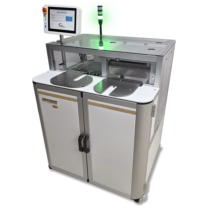
CEE Apogee Thermal Slide Debonder
Controlled thermal debonding for thin, sensitive and high-value substrates
The Cee® Apogee® Thermal Slide Debonder is a compact, semi-automated system designed to bring consistency, control and repeatability to wafer debonding processes. Developed for semiconductor, compound semiconductor, optical and advanced substrate applications, it uses controlled heat, vacuum and programmed slide-off motion to separate bonded wafer pairs safely and efficiently.
Designed for both R&D and production environments, the Apogee® Thermal Slide Debonder helps reduce the risks associated with manual debonding, including substrate breakage, process variation and operator-dependent results. It is particularly well suited to waxes and thermoplastic adhesives, enabling clean separation without the need for chemical baths or excessive manual handling.
With dual heated platens, programmable recipe control, DataStream™ process logging and support for substrate sizes from 2 inch to 200 mm, the system gives users a practical route to more controlled, traceable and repeatable debonding workflows.
Product synopsis
The Apogee® Thermal Slide Debonder has been developed to eliminate process variability and reduce manual debonding risk, combining semi-automated wafer loading and unloading with a fully automated debond sequence. It supports a wide range of adhesives, wafer sizes and process scales, making it a flexible tool for laboratories, pilot lines and production environments.
Key capabilities include:
- Semi-automated wafer loading and unloading
- Fully automated debond sequence
- Dual heated platens
- Recipe-controlled substrate size changes
- Controlled thermal and slide-off separation
- Programmable force, speed, temperature and time
- Process logging and traceability for every wafer
- DataStream™ technology for real-time process visibility
- Compact, self-contained floor-standing format
- Support for 2 inch to 200 mm substrates
Key benefits
Reduced manual handling risk
Manual debonding can introduce avoidable variation and risk, especially when working with thin, fragile or high-value wafers. The Apogee® Thermal Slide Debonder helps minimise operator-dependent handling by automating the critical debonding sequence and providing controlled wafer loading and unloading.
Improved process repeatability
Recipe control allows key parameters such as temperature, force, speed and time to be defined, stored and repeated. This is particularly valuable where process stability, wafer-to-wafer consistency and traceability are important.
Gentle handling of sensitive substrates
The system is designed for low-stress debonding, with controlled slide force, vacuum management and failsafe force detection to help protect device wafers during separation.
Suitable for R&D and production
With estimated throughput of 8–14 wafers per hour for substrates up to 150 mm, and 4–8 wafers per hour for substrates up to 200 mm, the system can support process development, pilot-scale work and production use cases.
Built-in traceability
DataStream™ technology provides process logging, online graphical process charts, remote process management and upload/download of process parameters via USB and Ethernet.
How the thermal slide debonding process works
The Apogee® Thermal Slide Debonder uses a controlled thermal slide-off process to separate a bonded wafer pair. The bonded wafers are loaded carrier-side down and device-side up, then transferred onto the lower heated platen. The system applies vacuum to hold the substrate securely, aligns the lower platen beneath the upper platen, and brings the wafer pair into contact under controlled conditions.
Once the upper platen has secured the device wafer, the system performs the programmed slide motion using defined force, speed and travel length. The carrier wafer remains on the lower platen while the device wafer is retained by the upper platen. The carrier is returned to the load tray and the device wafer is transferred to a Gel Pak for removal.
This controlled process helps reduce the variability and handling risk typically associated with manual debonding, while giving users precise control over the parameters that influence separation quality.
Features and programmability
The Apogee® Thermal Slide Debonder includes a full-colour touchscreen graphical user interface, with recipe-based control of process parameters including temperature, force, speed and time. Users can create unlimited user-defined program steps for each recipe, with 0.1-second resolution for step timing.
Core programmable features include:
- Upper and lower platen temperature control
- Debond force and speed control
- Lift pin height and timing
- Substrate size settings
- Stack thickness and search distance
- Pre-debond delay and soak time
- Cool time after processing
- Vacuum checks and process preconditions
- Force and cycle-time logging
The system also includes manual control functions for process development, prototyping, system verification and recovery from aborted processes.
DataStream™ technology
DataStream™ technology connects Apogee® manufacturing equipment through a browser-based interface, allowing users to track, access and modify systems from one place. For the Thermal Slide Debonder, this provides valuable process visibility, data capture and recipe management capability.
DataStream™ supports:
- Real-time process monitoring
- Visual process status and health indicators
- Environmental monitoring of temperature and humidity
- Basic and advanced recipe creation
- Plain-English recipe translation
- Unlimited recipe storage
- Data logging and export
- Process troubleshooting and optimisation
- Best-known method development
For facilities working across multiple Apogee® tools, DataStream™ can help create a more connected, traceable and consistent process environment.
Typical applications
The Apogee® Thermal Slide Debonder is intended for semiconductor and optical applications, particularly where bonded substrates need to be separated cleanly and repeatably after thinning, processing or temporary bonding workflows.
Typical applications include:
- Temporary wafer bonding and debonding workflows
- Compound semiconductor processing
- Thin wafer handling
- Substrate separation after thermal processing
- Wax and thermoplastic adhesive debonding
- R&D process development
- Pilot production and process transfer
- Advanced packaging and device wafer handling
- Optical substrate processing
Substrate and wafer compatibility
The Apogee® Thermal Slide Debonder supports substrate sizes from 2 inch to 200 mm and is suitable for a broad range of wafer and substrate materials. Qualified wafer materials include SiC, GaN, GaAs, InP, sapphire, silicon, glass and more.
The system is optimised for waxes and thermoplastic adhesives and is designed to support clean, controlled separation without chemical baths. This makes it especially useful for sensitive materials and thin substrates where repeatable, low-stress handling is essential.
Technical specifications
| Specification | Detail |
|---|---|
| Substrate sizes | 2 inch to 200 mm |
| Maximum temperature | 300°C |
| Temperature uniformity | 0.3% across working surface |
| Platen control | Independent upper and lower platen temperature controls |
| X-axis debond force | 1 to 100 N |
| X-axis force resolution | 1 N |
| X-axis maximum velocity | 20 mm/s |
| Z-axis resolution | 1 micron |
| Safety | Failsafe Z-axis force detection |
| Throughput | Est. 8–14 WPH for ≤150 mm; est. 4–8 WPH for ≤200 mm |
| System uptime | >99% over a 12-month period |
| MTTR | <24 hours |
| MTBF | >600 hours / 6,000 cycles |
| Warranty | 1-year full warranty on parts and labour |
Utilities and installation requirements
The Apogee® Thermal Slide Debonder is a compact, self-contained floor-standing unit designed for clean, climate-controlled environments. It requires a level floor and standard facility connections for power, vacuum, exhaust and nitrogen or clean dry air.
| Requirement | Detail |
|---|---|
| Dimensions | 38.7” / 983 mm W x 40.2” / 1022 mm D x 57” / 1448 mm H |
| Machine weight | 560 lb / 208.7 kg, excluding accessories |
| Voltage range | 208–230 VAC |
| Power requirement | 15.3 A maximum |
| Vacuum | 1/4” push-to-connect, <20” Hg / 33 kPa |
| Exhaust | 2” OD, 0.4” H₂O @ 10 CFM / 100 Pa @ 17 CMH |
| N₂ / CDA | 1/4” push-to-connect, 70 psi / 482 kPa |
Designed for reliability and support
CEE has served the semiconductor industry since 1987, and the Apogee® Thermal Slide Debonder has been developed with reliability, serviceability and long-term support in mind. The system is supplied with a one-year full warranty on parts and labour, along with complimentary remote technical support and application process assistance for the life of the product.
For production environments, the combination of compact footprint, high uptime, process logging and controlled recipes makes the system a practical alternative to manual debonding methods where consistency and wafer protection are critical.
Why choose SiSTEM Technology?
SiSTEM Technology supports CEE customers across the UK and Europe, helping research institutions, semiconductor facilities and advanced manufacturing teams identify the right equipment for their process requirements.
Our team can support you with:
- Initial product selection
- Technical discussions with CEE
- Process and application guidance
- Quotation and procurement support
- Installation coordination
- Training and after-sales support
- Long-term supplier communication
Whether you are developing a new temporary bonding process, improving an existing manual debonding workflow, or looking to add controlled wafer separation capability to your lab or production line, SiSTEM Technology can help you explore whether the Apogee® Thermal Slide Debonder is the right fit.
Enquire about the Cee® Apogee® Thermal Slide Debonder
To discuss your wafer debonding process, substrate materials or production requirements, contact SiSTEM Technology. We can help you review the technical specification, discuss compatibility with your process, and arrange further information from CEE where required.