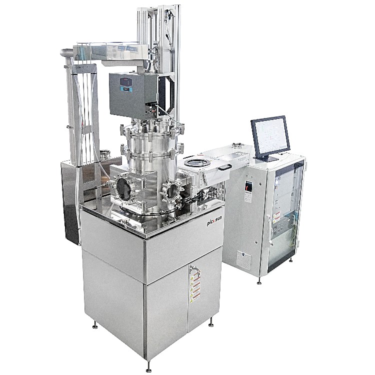
R-200 Advanced
Introducing the versatile PICOSUN® R-200 Advanced atomic layer deposition systems, perfect for research and development across a wide spectrum of applications. Whether you’re working with IC components, MEMS devices, displays, LEDs, lasers, or 3D objects like lenses, optics, jewellery, coins, or medical implants, these systems provide the ideal platform for exploration and innovation. Unleash your creativity and unlock the full potential of atomic layer deposition technology with the PICOSUN® R-200 Advanced ALD systems.
With its agile design, the PICOSUN® R-200 Advanced ALD system offers unparalleled quality in ALD film depositions while providing ultimate system flexibility to meet future needs and applications. Featuring Picosun’s patented hot-wall design with fully separated inlets and instrumentation, it ensures particle-free processing on a diverse range of materials, including wafers, 3D objects, and nanoscale features. Even the most challenging samples with through-porous structures, ultra-high aspect ratios, and nanoparticles achieve excellent uniformity, thanks to the proprietary Picoflow™ technology.
Equipped with highly functional and easily interchangeable precursor sources for liquid, gaseous, and solid chemicals, the PICOSUN® R-200 Advanced systems offer remarkable efficiency. Additionally, the patented remote plasma option enables the deposition of metals without the risk of short-circuiting or plasma damage. The system seamlessly integrates with glove boxes, UHV systems, manual and automated loaders, cluster tools, powder chambers, roll-to-roll chambers, and various in situ analytics systems, empowering efficient and flexible research across diverse domains. No matter your current research area or what it may evolve into in the future, the PICOSUN® R-200 Advanced atomic layer deposition system ensures optimal results for your endeavors.