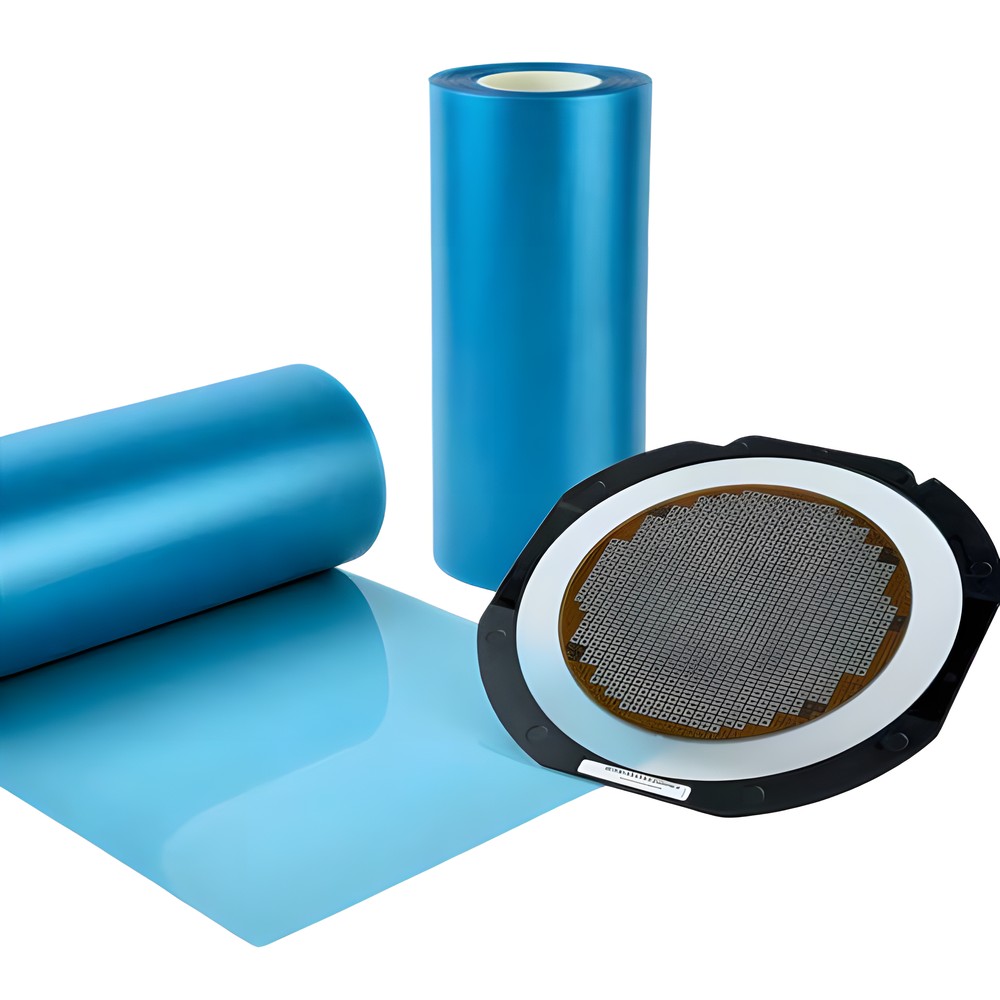
Back-Grinding and Bump Tape
Back-grinding and bump tape for wafer thinning
D&X back-grinding tape covers the patterned front face of a wafer while its back is ground down. It holds strongly enough to keep grinding water and debris out, sits flat for an even grind, and peels away without residue. D&X’s bump tape does the same job on bumped wafers. Both are made in Japan. Our wafer dicing and back-grinding tape page covers the choice between UV and non-UV.
Back-grinding tape
The standard tapes are compatible with conventional back-grinding processes and run from 130 µm to 200 µm thick on a PO base film. The UV types combine high tape thickness accuracy with easy peeling, even on thin wafers, because UV exposure releases the adhesive before the tape comes off. The non-UV types cover general-purpose work, with higher-adhesion versions available.
Bump tape
Bumped wafers need a tape that closes around the bumps and protects them. DX-LCP290Z carries a 140 µm adhesive layer on a 150 µm base, and D&X designs its bump tapes to handle a range of bump sizes, heights and pitches without residue or damage to the bumps. They also give heat resistance and long-term protection of the film.
| Tape | Type | Thickness (µm) | Base / adhesive (µm) | Adhesion before / after UV (mN/25 mm) |
|---|---|---|---|---|
| DX-LCP180K | UV | 180 | PO 150 / urethane 30 | 18,000 / 100 |
| DX-LCP130GX | UV | 130 | PO 100 / urethane 30 | 13,500 / 90 |
| DX-LCP130GNX | Non-UV, general purpose | 130 | PO 100 / acrylic 30 | 1,200 |
| DX-LCP180LNX | Non-UV, higher adhesion | 180 | PO 150 / acrylic 30 | 1,400 |
| DX-LCP200LNX | Non-UV, higher adhesion | 200 | PO 150 / acrylic 50 | 1,900 |
| DX-LCP290Z | UV, bumped wafers | 290 | PO 150 / acrylic 140 | 22,000 / 190 |
Width, length, thickness, hardness and adhesion can be specified to suit your grinder and wafer.
Key features and benefits
- UV and non-UV back-grinding tapes from 130 µm to 200 µm
- High tape thickness accuracy for an even grind
- UV release for easy peeling on thin wafers
- Bump tape for bumped wafers, with a 140 µm adhesive layer
- No adhesive residue on the wafer or bumps
- Made in Japan, inspection sheet with every shipment
- Short rolls to full production quantities
To ask for samples or a quotation, contact us or request a quote.