

CZ silicon wafers from 2″ to 12″ in test, monitor and prime grades, shipped from stock, plus custom thickness, resistivity, orientation and film-coated wafers.

D&X: semiconductor wafers, substrates and wafer tape from Japan
D&X makes and supplies the materials a wafer process starts with and the tape that carries it through grinding and dicing. The company was founded in 2008 and is based in Tokyo, with offices in Taiwan, Germany and China, more than 100 staff and more than 500 customers worldwide. Its tape is made in Japan at a production facility D&X opened in 2023, and the business holds ISO 9001:2015 and ISO 14001:2015 certification. SiSTEM Technology supplies D&X wafers and tape in the UK and Ireland.
Alongside our equipment and consumables
Most of the equipment we supply needs wafers to run, from the day it’s qualified onwards. D&X holds a large stock of standard wafers, takes small orders, and can grow or source the unusual ones. It sits naturally alongside the spares and consumables we already handle.
Silicon wafers from stock
D&X carries silicon wafers from 2″ to 12″ in test, monitor and prime grades, ready to ship from single cassettes up to orders of more than 10,000 wafers. Standard specifications ship straight from stock, and D&X says most custom specifications are processed and shipped within four weeks. Beyond the standard sizes it can supply ingots and coinroll wafers from 1″ to 18″, thicknesses from 5 µm to over 2,000 µm, resistivity from 0.001 to 20,000 ohm-cm, and particle-controlled wafers for 200 mm and 300 mm tools. Film-coated wafers carry oxide, nitride, PE-TEOS or metal films.
SiC, compound and specialty substrates
For power and RF work, D&X supplies silicon carbide in 4H and 6H polytypes, conductive and semi-insulating, graded by micropipe density from zero-MPD through to dummy. Gallium arsenide, indium phosphide, gallium nitride and germanium complete the compound range. Specialty substrates cover SOI with the device layer, buried oxide and handle all specified to order, sapphire in C, R, M and A planes, crystal quartz in the common cuts, and glass wafers from 50 mm to 300 mm in borosilicate, fused silica, BK7, Eagle XG and soda lime.
Dicing, back-grinding and bump tape
D&X tape covers the back end of the wafer’s life. The dicing tapes are UV and non-UV types for silicon, glass, ceramics and packaging substrates, with antistatic and RoHS 2.0 compliant options. Back-grinding tapes protect the front face while the wafer is thinned, and bump tapes carry bumped wafers through grinding without damaging the bumps. Width, length, thickness, adhesion and hardness can all be specified, quantities run from short rolls to full production, and every shipment comes with an inspection sheet.
Working with us
We handle enquiries, quotations and orders for D&X wafers and tape in the UK and Ireland, and bring in D&X’s own team when a specification needs their input. Tell us the material, the diameter, the grade and what the wafer has to do in your process, and we’ll come back with what D&X has in stock and what would need to be made. If a substrate is outside the range, we’ll say so.
D&X products
Silicon wafers
Test, monitor and prime grades, 2″ to 12″, from stock.
SiC and compound semiconductor wafers
SiC, GaAs, InP, GaN and germanium.
Specialty substrates
SOI, sapphire, quartz and glass.
Dicing tape
UV and non-UV, for silicon, glass and packaging substrates.
Back-grinding and bump tape
Wafer protection through thinning, including bumped wafers.
Contact us to discuss a specification, ask what’s in stock, or request a quotation.
Stock Wafers, Small Orders
Standard silicon wafers ship from stock, from a single cassette upwards. That suits research groups and process development work, where 25 test wafers matter more than 25,000.Specifications Beyond the Catalogue
Thickness from 5 µm to over 2,000 µm, resistivity from 0.001 to 20,000 ohm-cm, and <100>, <110> or <111> orientation. D&X says most custom silicon specifications ship within four weeks.Compound and Specialty Substrates
SiC in 4H and 6H, GaAs, InP, GaN and germanium, plus SOI, sapphire, quartz and glass. One source for the substrates a mixed research lab or a pilot line tends to need.Tape Made in Japan
D&X makes its own dicing, back-grinding and bump tape, and opened a dedicated tape manufacturing facility in 2023. Each shipment comes with an inspection sheet.Certified Quality
D&X holds ISO 9001:2015 and ISO 14001:2015 certification.Ordered Through the UK
We handle enquiries, quotations and orders in the UK and Ireland, so you deal with a local contact in your own time zone and D&X's team is brought in when a specification needs it.-
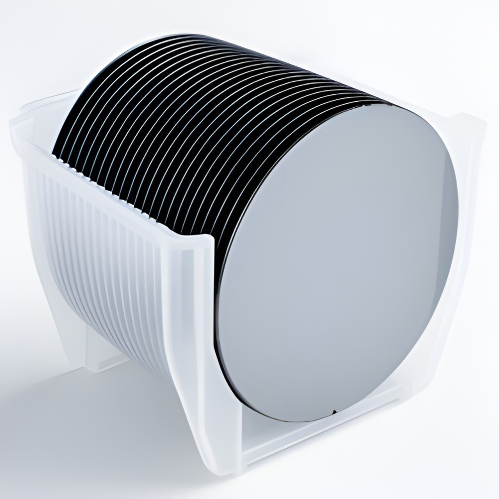
Silicon Wafers - Test, Monitor and Prime Grades
-
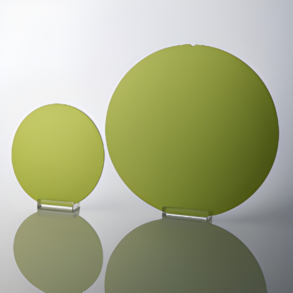
SiC and Compound Semiconductor Wafers
Silicon carbide wafers in 4H and 6H polytypes, graded by micropipe density, plus gallium arsenide, indium phosphide, gallium nitride and germanium substrates.
-
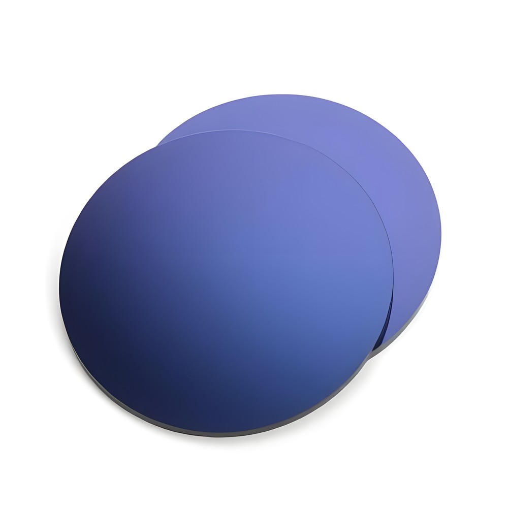
Specialty Substrates - SOI, Sapphire, Quartz and Glass Wafers
Silicon-on-insulator, sapphire, crystal quartz and glass wafers made to specification, for MEMS, photonics, optics and packaging.
-
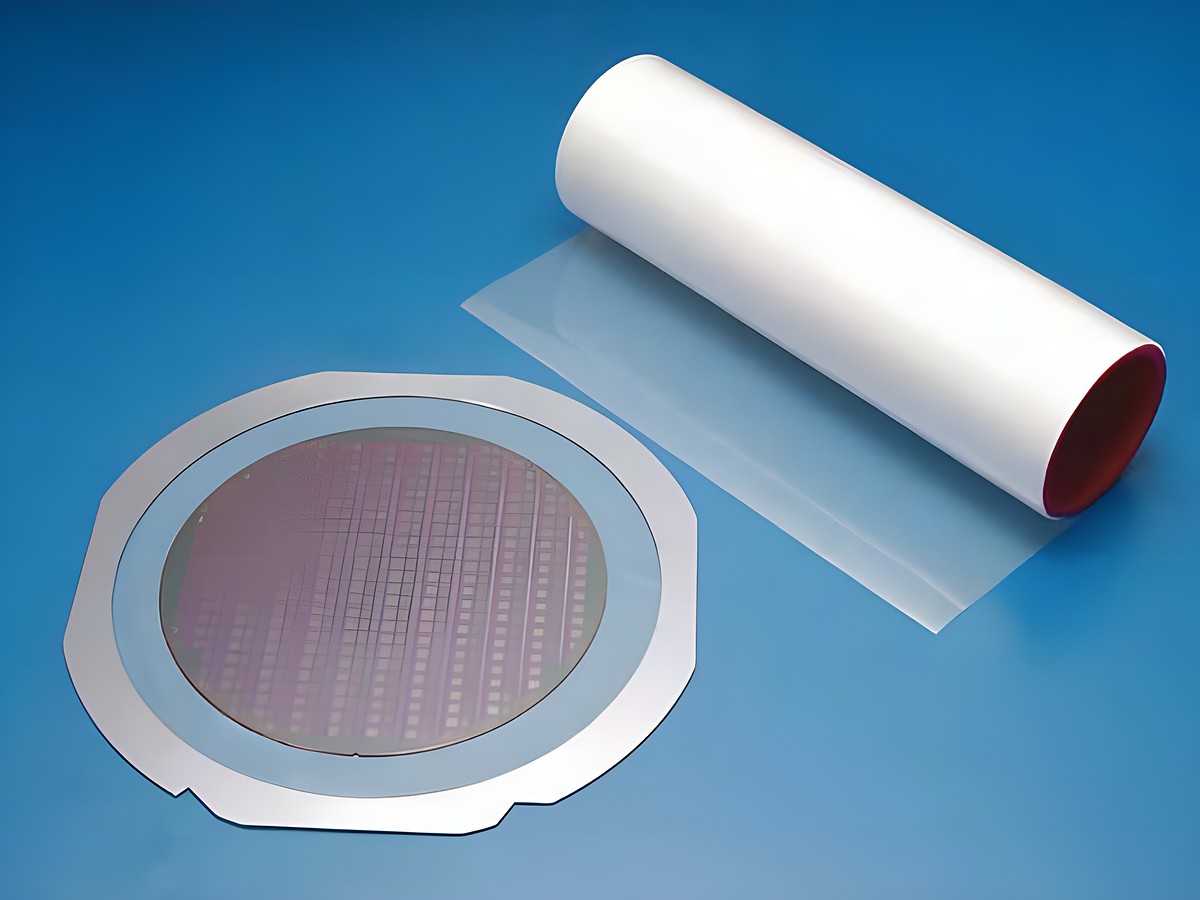
Dicing Tape - UV and Non-UV
UV and non-UV dicing tape for silicon wafers, glass, ceramics and packaging substrates, made in Japan with an inspection sheet on every shipment.
-
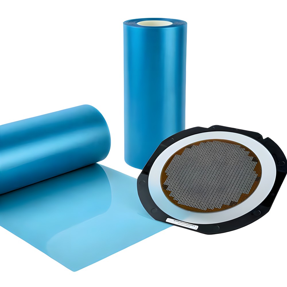
Back-Grinding and Bump Tape
UV and non-UV back-grinding tape with high thickness accuracy, and bump tape for bumped wafers, protecting the front face during wafer thinning.