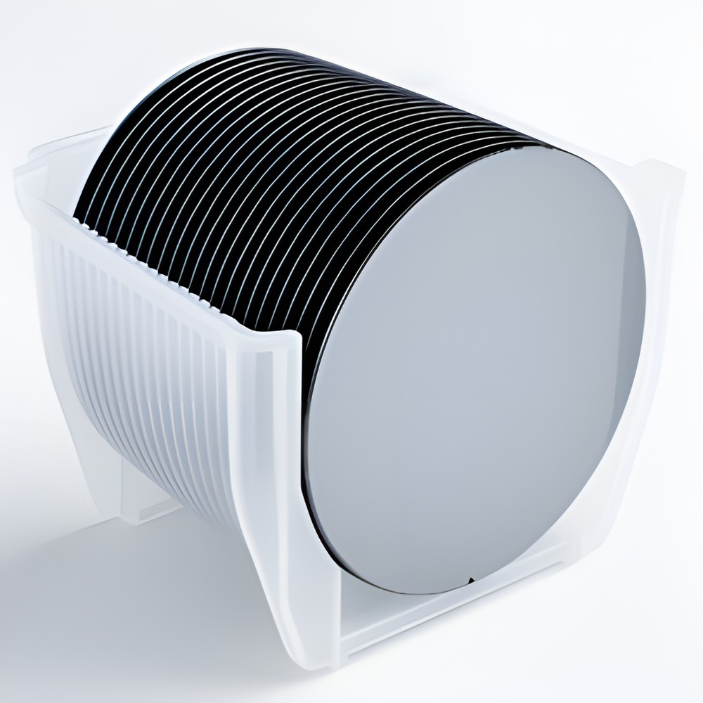
Silicon Wafers - Test, Monitor and Prime Grades
Silicon wafers from stock, in any quantity
D&X holds silicon wafers from 2″ to 12″ in stock, in test, monitor and prime grades, and ships them from a single cassette up to orders of more than 10,000 wafers. They’re used for tool qualification, process monitoring, recipe development and device work in semiconductor fabs and research and development labs. Our semiconductor wafers and substrates page covers the rest of the range.
Standard specification
Standard wafers are CZ-grown, P or N type, polished or etched, with SEMI flats up to 6″ and a notch on 12″. Test grade wafers hold TTV at 10 µm or better, bow and warp below 40 µm, and 10 particles or fewer at 0.3 µm.
| Diameter | Standard thickness | Flat / notch |
|---|---|---|
| 2″ | 280 ± 25 µm | Flat |
| 3″ | 380 ± 25 µm | Flat |
| 4″ | 525 ± 25 µm | Flat |
| 5″ | 625 ± 25 µm | Flat |
| 6″ | 625 or 675 ± 25 µm | Flat |
| 8″ | 725 ± 25 µm | Flat or notch |
| 12″ | 775 ± 25 µm | Notch |
Surface finishes are as-cut, lapped, etched, single-side polished or double-side polished.
Particle-controlled wafers for 200 mm and 300 mm
For particle monitoring on 200 mm and 300 mm tools, D&X supplies particle-controlled wafers at thresholds from 200 nm down to 15 nm. At 300 mm these hold thickness to 775 ± 5 µm, with TTV down to 1 µm or better on the tightest grade.
Custom specifications
Outside the standard list, D&X can supply thicknesses from 5 µm to over 2,000 µm, resistivity from 0.001 to 20,000 ohm-cm, and <100>, <110> or <111> orientation, as ingots, coinroll wafers from 1″ to 18″, or finished wafers. D&X says most custom specifications are processed and shipped within four weeks. Deliveries can also be scheduled monthly, quarterly or annually for longer programmes.
Film-coated wafers
Wafers can be supplied with oxide (SiO2), nitride (Si3N4), PE-TEOS, or metal films including aluminium, nickel, titanium, copper and titanium nitride, for deposition, etch and CMP monitoring.
Key features and benefits
- 2″ to 12″ silicon wafers in test, monitor and prime grades
- Standard specifications shipped from stock, from a single cassette upwards
- Particle-controlled 200 mm and 300 mm wafers, down to 15 nm
- Thickness from 5 µm to over 2,000 µm, resistivity from 0.001 to 20,000 ohm-cm
- <100>, <110> and <111> orientation
- As-cut, lapped, etched, SSP and DSP finishes
- Oxide, nitride, PE-TEOS and metal film-coated wafers
- Monthly, quarterly or annual delivery schedules
To ask what’s in stock or request a quotation, contact us or request a quote.