

CZ silicon wafers from 2″ to 12″ in test, monitor and prime grades, shipped from stock, plus custom thickness, resistivity, orientation and film-coated wafers.
Semiconductor wafers and substrates
Every process starts with a wafer, and most of the equipment we supply needs a steady flow of them for qualification, monitoring and development work. SiSTEM Technology supplies wafers and substrates from D&X in the UK and Ireland, from stock silicon wafers through to substrates grown or cut to your specification.
Choosing a wafer
A wafer specification comes down to a handful of choices. Material and diameter come first, then growth method, orientation, doping and resistivity, then thickness and surface finish, with flatness held as tightly as the process needs. Grade decides how much of that has to be held tightly. A dummy wafer for tool set-up needs almost none of it; a prime wafer for device work needs all of it, plus a particle count.
Most of the wafers a lab gets through are test and monitor wafers, used to qualify a tool, check a recipe or measure a film. They’re where a large stock and a small minimum order pay off, because the need is frequent and the quantities are modest.
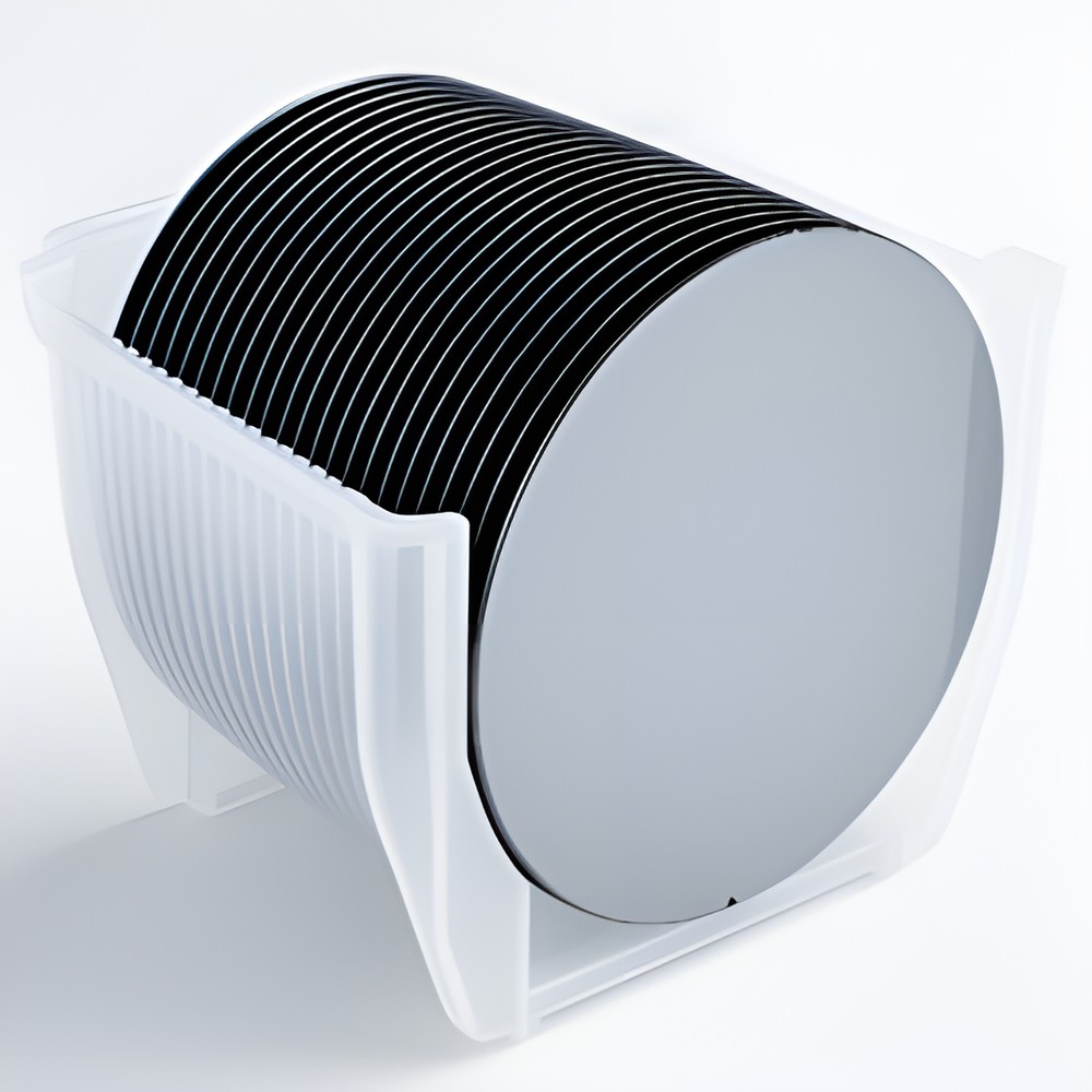
Silicon wafers
D&X holds silicon wafers from 2″ to 12″ in test, monitor and prime grades, CZ-grown, P or N type, with standard SEMI thicknesses from 280 µm at 2″ to 775 µm at 12″. Finishes run from as-cut and lapped to etched, single-side polished and double-side polished. Standard wafers ship from stock, and D&X says most custom specifications ship within four weeks.
For 200 mm and 300 mm tools there are particle-controlled wafers with particle specifications down to 15 nm. At the other end, D&X can supply non-standard thicknesses from 5 µm to over 2,000 µm, resistivity from 0.001 to 20,000 ohm-cm, and <100>, <110> or <111> orientation. Film-coated wafers carry oxide, nitride, PE-TEOS or metal films for deposition and etch monitoring.
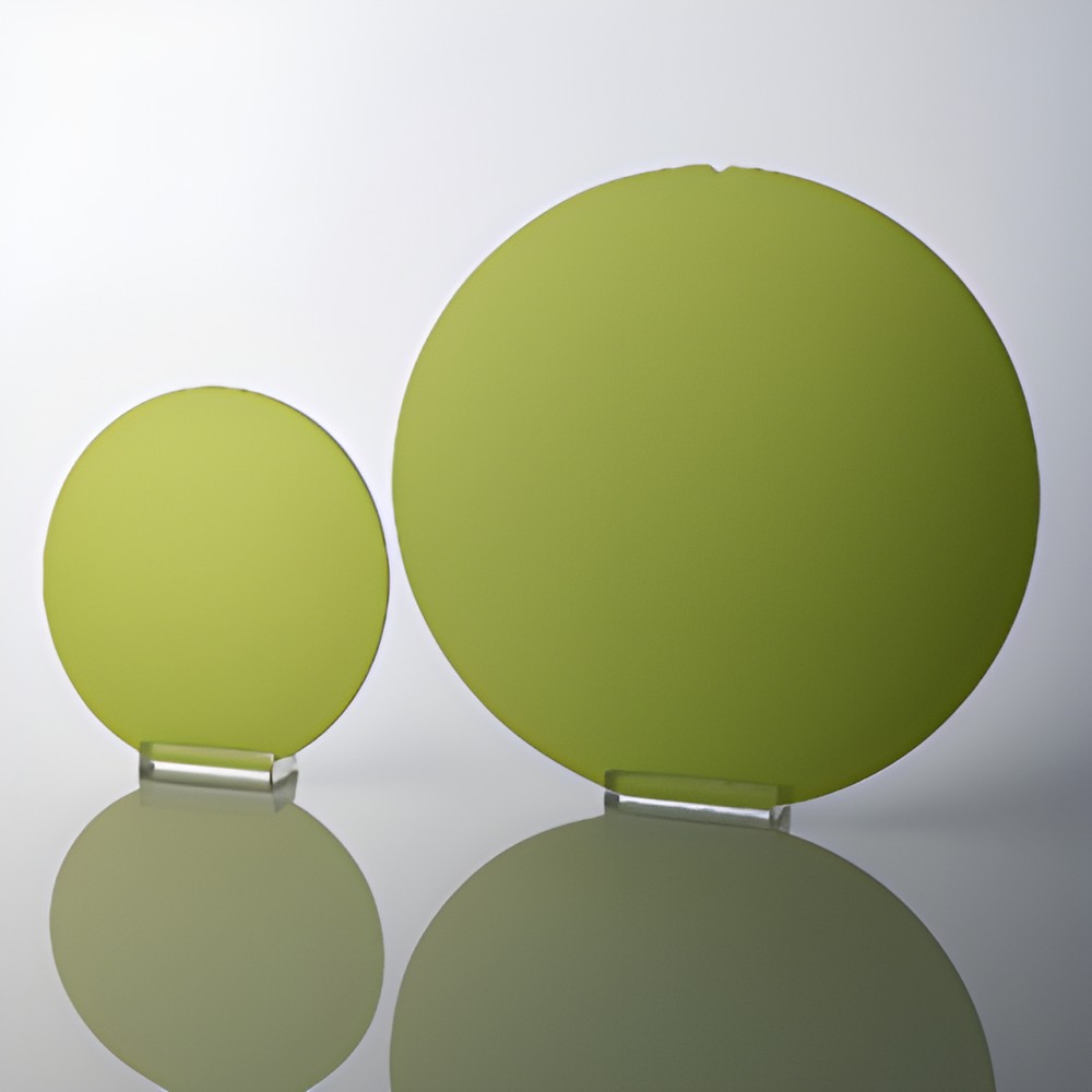
Silicon carbide and compound semiconductors
SiC and compound semiconductor wafers cover power, RF and optoelectronic work. Silicon carbide comes in 4H and 6H polytypes, conductive or semi-insulating, graded by micropipe density from zero-MPD for device work through production and research grades to dummy wafers for tool set-up. Gallium arsenide, indium phosphide, gallium nitride and germanium complete the range.
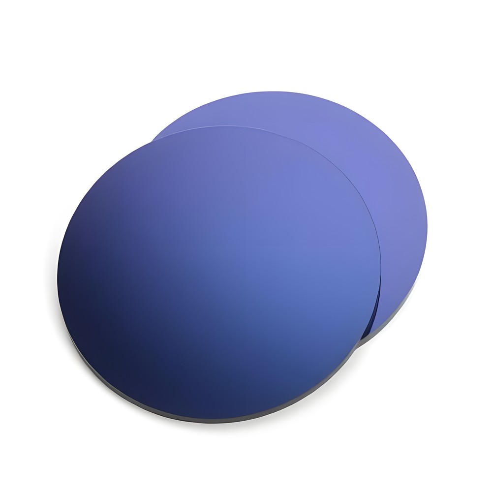
Specialty substrates
SOI, sapphire, quartz and glass are made to order. SOI is specified layer by layer, from the device layer through the buried oxide to the handle. Sapphire comes in C, R, M and A planes up to 200 mm, crystal quartz in the standard cuts including AT and ST, and glass wafers in borosilicate, fused silica, BK7, Eagle XG and soda lime from 50 mm to 300 mm. Glass and silicon wafers are the usual carriers in temporary bonding, which we also support.
After the wafer
Once a wafer has been processed, it usually needs protecting while it’s thinned and holding while it’s diced. D&X makes the tape for both, covered on our wafer dicing and back-grinding tape page.
Getting a quotation
Send us the material, diameter, grade and quantity, along with any orientation, resistivity or thickness requirement, and tell us what the wafers are for. We’ll check what D&X has in stock, what would need to be made and how long each takes. For samples and small quantities, ask; small orders are a large part of why we work with D&X.
Wafer and Substrate Products
-
Silicon Wafers - Test, Monitor and Prime Grades
-
SiC and Compound Semiconductor Wafers
Silicon carbide wafers in 4H and 6H polytypes, graded by micropipe density, plus gallium arsenide, indium phosphide, gallium nitride and germanium substrates.
-
Specialty Substrates - SOI, Sapphire, Quartz and Glass Wafers
Silicon-on-insulator, sapphire, crystal quartz and glass wafers made to specification, for MEMS, photonics, optics and packaging.