

UV and non-UV dicing tape for silicon wafers, glass, ceramics and packaging substrates, made in Japan with an inspection sheet on every shipment.
Wafer dicing and back-grinding tape
Two steps near the end of a wafer’s life depend on tape. Back-grinding tape protects the patterned front face while the wafer is thinned, and dicing tape holds the wafer on its frame while it’s cut into dies and keeps those dies in place for pick-up. SiSTEM Technology supplies tape from D&X in the UK and Ireland. D&X makes it in Japan, at a tape manufacturing facility it opened in 2023.
UV or non-UV
The first choice with either tape is how it lets go. UV-curable tapes hold strongly during grinding or dicing, then lose most of their adhesion under UV exposure, so thin wafers and small dies come away cleanly. On D&X’s standard silicon dicing tape, adhesion drops from 6,500 to 260 mN/25 mm after UV. Non-UV tapes peel at a fixed, lower adhesion and suit general-purpose work where the extra step isn’t needed.
Dicing tape
D&X dicing tape covers silicon wafers, glass and ceramics, and packaging substrates. The silicon tapes are thin PVC-based films that expand evenly for die separation, with transparent, antistatic and RoHS 2.0 compliant versions. Packaging substrate tapes use PO, PET or EVA base films with stronger adhesives, for hard-to-cut and uneven surfaces. D&X designs them to reduce chipping and prevent whiskers, with no adhesive residue left on the die.
Back-grinding and bump tape
Back-grinding and bump tape holds the wafer flat and keeps grinding water and debris off the front face. The standard tapes run from 130 µm to 200 µm thick on PO base film, in UV and non-UV versions, with high thickness accuracy for an even grind. Bumped wafers need a tape that conforms around the bumps without damaging them, and D&X’s bump tape, 290 µm thick with a 140 µm adhesive layer, is built for that.
Made to your process
Tape width, length, thickness, hardness and adhesion can all be specified. Quantities run from short rolls for a trial to full production supply, and every shipment comes with an inspection sheet. D&X can supply samples for evaluation before an order.
Getting a quotation
Tell us the wafer or substrate material, its thickness and diameter, whether it’s bumped, the frame or tape width you use, and your dicing or grinding method. We’ll suggest the D&X tapes that fit and arrange samples if you’d like to test them first.
If you need the wafers as well, see semiconductor wafers and substrates.
Dicing and Back-Grinding Tape Products
-
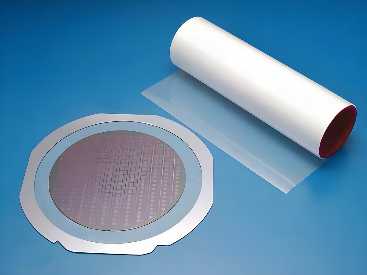
Dicing Tape - UV and Non-UV
-
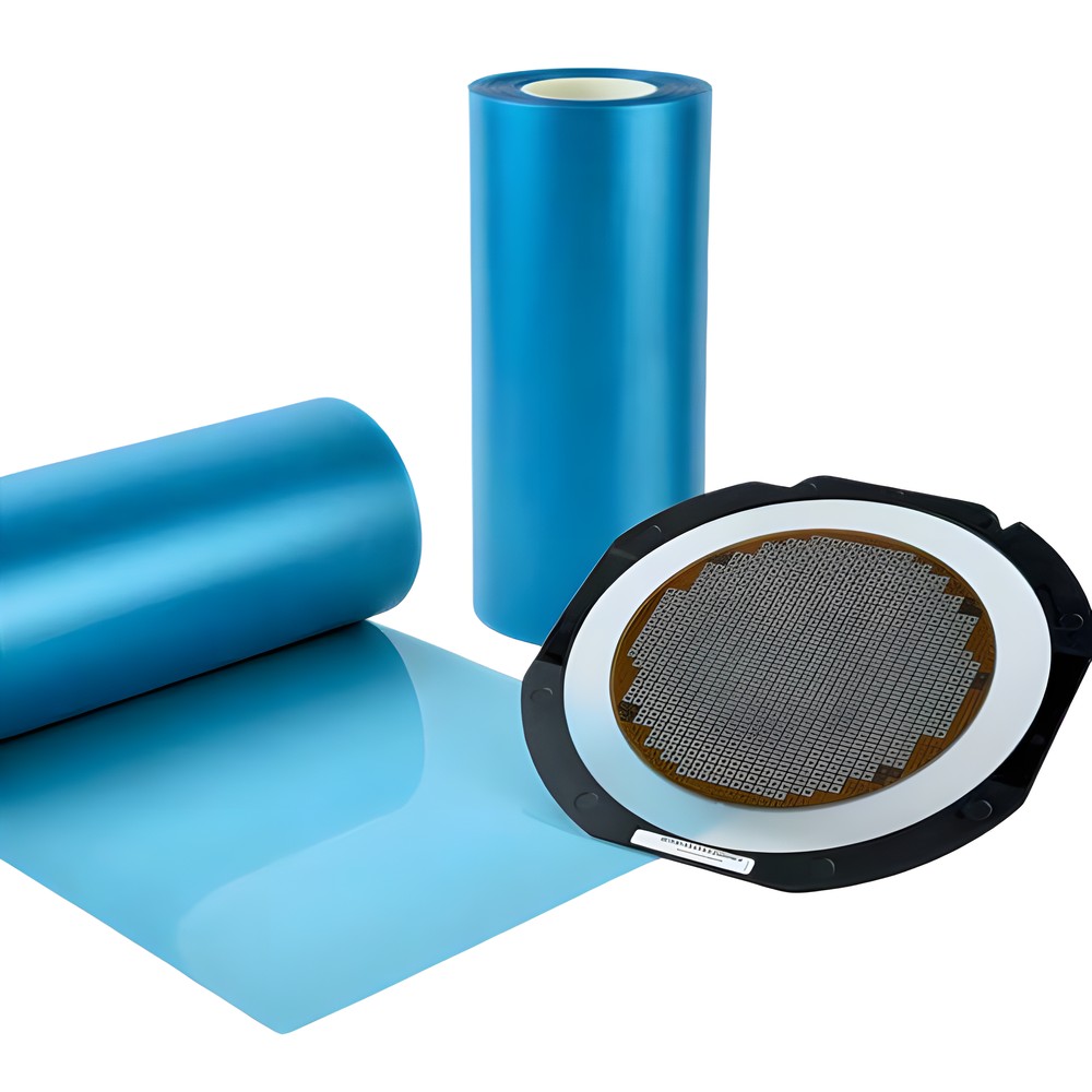
Back-Grinding and Bump Tape
UV and non-UV back-grinding tape with high thickness accuracy, and bump tape for bumped wafers, protecting the front face during wafer thinning.
-
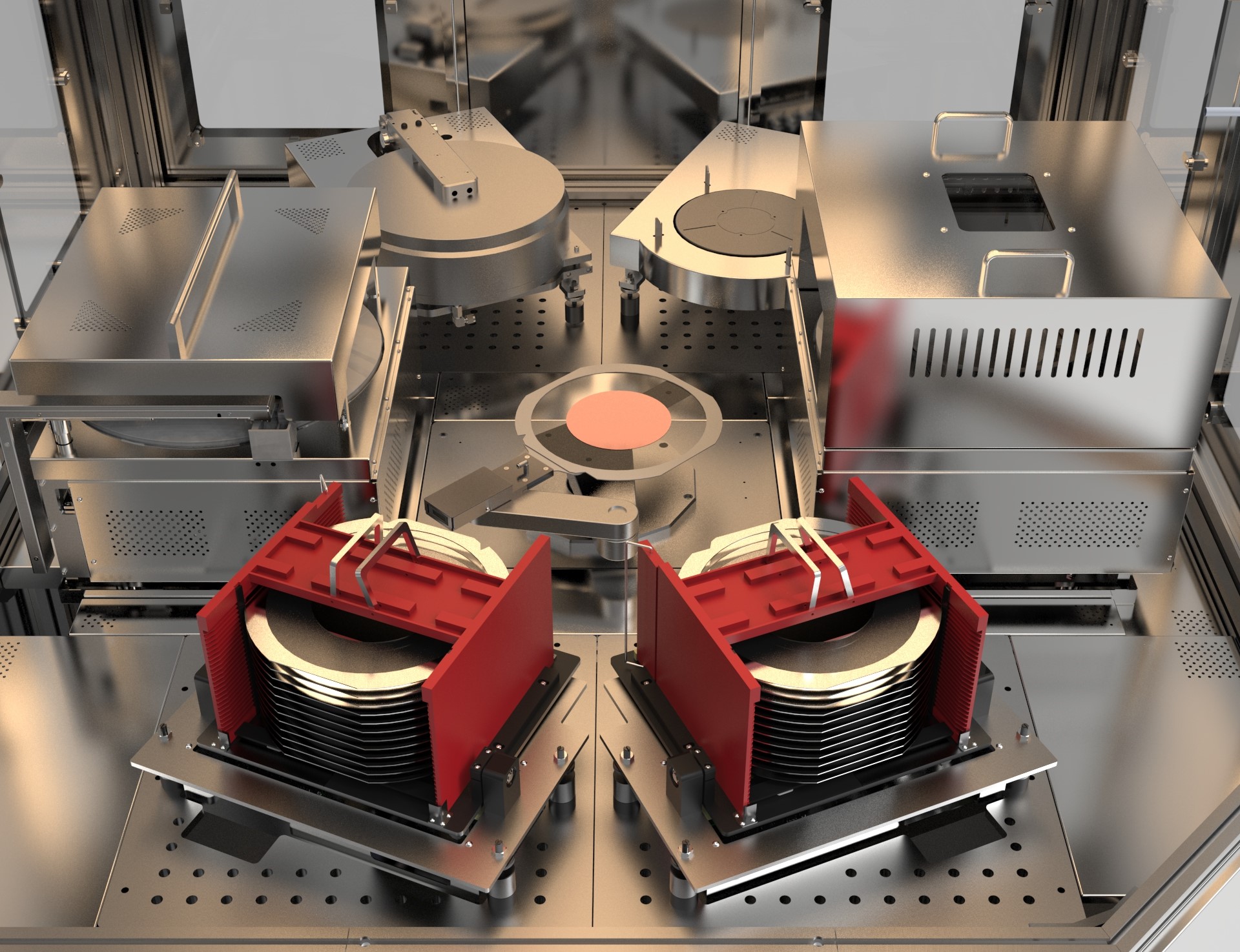
P9000-30 Frame Processing System
- Protective coating before saw or laser scribe
- Wafer and frame cleaning after dicing
- 50mm to 300mm wafers on frames, down to 50 µm thick
- Manual or automatic loading