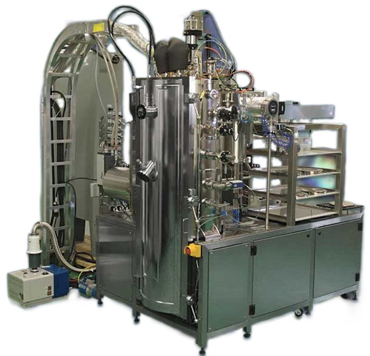
- Indium bump deposition on wafers up to 200 mm
- Full 4 µm indium run in under 2.5 hours
- Automatic or manual load lock with in-situ pre-clean
- Wafer temperature control from +60°C to -75°C
- Hundreds of depositions without opening the main chamber
Email: info@sistemtechnology.com Call: +44 (0)1327 362 844


Indium Bump Deposition for Flip-Chip Bonding
Indium bumps are the small metal pillars that join two chips face to face in flip-chip bonding. Typical pairs are an infrared detector array and its readout circuit, or a quantum device and its carrier. Indium is ductile and melts at 156.6°C, so bonding stays gentle on temperature-sensitive parts. It also conducts heat well and works with III-V and II-VI semiconductors. Intlvac Thin Film builds the Icarus, a production system for evaporating indium bumps. SiSTEM is Intlvac’s partner for the UK, Ireland and most of Europe.
How evaporated bumps are made
Evaporated bumps are usually formed by lift-off. Indium is evaporated over a wafer patterned with photoresist, and when the resist is stripped it takes the unwanted indium with it, leaving bumps on the pads.
Lift-off depends on a flat, uniform deposition front and a directional, collimated flux of indium. The Icarus gets both from its long throw between source and wafer, and its thickness and fill can be set to suit the bump design.
Evaporation and electroplating
Indium bumps can also be electroplated. Intlvac’s view is that long-throw evaporation gives better adhesion, density, purity and thickness control, and suits a wider range of materials. The right route depends on your pitch, bump height and volumes, and we’re happy to talk it through.
Getting good bumps
Spitting is the main defect risk: droplets thrown from the source land on the wafer. Intlvac purifies the indium to stop it, and the Icarus evaporates from its Helios source, a large, thick-walled molybdenum crucible that holds a very stable rate over a long life.
Bump strength depends on temperature. Depositing onto a cold wafer improves shear strength, and on the Icarus the wafer is thermally bonded to its carrier for temperature control from +60°C down to -75°C. Before deposition, a cleaning position in the load lock removes light surface contamination, oxides and water vapour without etching the wafer.
Where indium bumps are used
Intlvac lists these uses for evaporated indium:
- infrared focal plane arrays
- quantum computing devices
- flip-chip bonding and semiconductor packaging
- microprocessors and integrated circuits
- ohmic contacts on III-V and II-VI semiconductors
- devices that need to shed heat efficiently
The Intlvac Icarus
The Icarus takes wafers of any size and shape up to 200 mm, on carriers made to suit the product. A 200 mm wafer takes under 120 minutes from start to finish, and the system runs hundreds of depositions without opening the main chamber. When the crucible needs refilling, it’s swapped for a pre-charged one in a few minutes. The Icarus page has the full detail.
Scoping an indium bump system
To put an Icarus together with Intlvac, we’ll ask about:
- your wafer sizes and shapes
- bump height, diameter and pitch
- your lift-off resist process
- the wafer temperature you need during deposition
- how many wafers you need to run a week
Working with SiSTEM
SiSTEM is Intlvac’s partner for the UK, Ireland and most of Europe. We scope your system with you and Intlvac’s engineers, and stay your local contact through quotation, installation and after-sales. Tell us your wafer sizes and bump design, and we’ll take it to Intlvac.