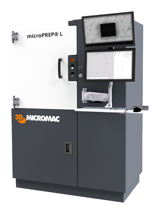
microPREP L Wafer- and Board-Level Laser Preparation System
microPREP L: laser preparation for full wafers and system-level boards
The 3D-Micromac microPREP L brings laser sample preparation to large substrates, from individual specimens up to full 300 mm wafers and system-level boards. 3D-Micromac launched it in November 2025 for semiconductor failure analysis, process development and quality assurance. Regions of interest are prepared directly on the substrate, which removes mechanical preparation steps and handling. Our sample preparation page covers the wider process.
Multi-site preparation in one run
Several regions of interest can be prepared within a single workflow without restarting the process. A multi-axis system positions, rotates and tilts the substrate without a dedicated handling setup for each task, and the system is prepared for automated semiconductor handling.
Feeding the rest of the lab
microPREP L takes over the slow coarse preparation for downstream tools such as FIB, BIB and plasma etching systems, and prepares samples for SEM, TEM, APT, optical microscopy, X-ray tomography and nanoCT. In 3D-Micromac’s benchmark tests, one operator prepared up to 32 samples a day, enough to feed up to seven plasma FIB systems. In another of their examples, a task that took 23 minutes on microPREP L would have taken up to six months by gallium FIB milling.
Controlled processing
A sealed process chamber is available for processing under vacuum, inert atmosphere or gas injection. Pico- and femtosecond pulses keep the heat-affected zone small, for controlled work on sensitive structures and complex material stacks. Contactless, non-abrasive cleaning options leave substrates ready for downstream analysis.
Targeted removal of defective structures
3D-Micromac also proposes microPREP L for removing individual defective elements from wafers, boards or devices while preserving the rest of the substrate for further production. They present it as an application idea, so it’s one to prove on your own material.
Key features and benefits
- Full 300 mm wafers and system-level boards, as well as individual specimens
- Multi-site preparation in one process run
- Multi-axis positioning, rotation and tilting
- Optional sealed process chamber
- Prepared for automated semiconductor handling
- Hardware and software adaptable to specific requirements
- Contactless, non-abrasive cleaning options
To discuss your substrates or arrange a trial at 3D-Micromac’s application laboratory in Chemnitz, contact us or request a quote.