

Laser sample preparation for TEM, FIB/SEM, atom probe and micromechanical testing, using pico- or femtosecond sources and standard stubs and mounts.

3D-Micromac: laser micromachining for semiconductor, microdiagnostics and display manufacturing
3D-Micromac builds laser machines for work that’s too fine, too brittle or too valuable for a mechanical tool. The company has been doing it since 2002 from Chemnitz in Germany, where around 200 staff have put more than 650 systems into semiconductor fabs, failure analysis labs, display plants and solar production lines. SiSTEM Technology represents 3D-Micromac in the UK and Ireland.
Why we took them on
Laser processing keeps turning up at the edges of our customers’ processes. A specimen has to reach a TEM without mechanical damage. Contacts on a SiC wafer need annealing without heating the device underneath. A 40 µm wafer would shatter under a blade. 3D-Micromac makes the machines that handle those jobs directly, and the range sits alongside the thin film, wafer handling and wet processing equipment we already supply, so a lab can build a workflow from one supplier.
Sample preparation for TEM, FIB and atom probe
The microPREP family prepares specimens for TEM, SEM and FIB cross-sections, atom probe tomography, X-ray tomography and micromechanical testing. Ultra-short laser pulses in the pico and femtosecond range keep the heat-affected surface to a few hundred nanometres or less, so metals, semiconductors, ceramics, polymers and compound materials can all be cut without the damage a mechanical route would leave.
The practical gain is time. Coarse material removal moves off the FIB and onto the laser, which leaves the FIB to do the fine work it’s actually for. 3D-Micromac describes microPREP as complementing ion beam preparation rather than replacing it.
microPREP PRO handles individual specimens on standard stubs and mounts. microPREP L takes full 300 mm wafers and system-level boards, with a sealed chamber available for vacuum, inert atmosphere or gas injection. The PRO FEMTO variant, which won a Laser Focus World Innovators Award in 2024, prepares atom probe cards with each pillar individually specified.
Laser annealing for power devices and magnetic sensors
microPRO XS OCF forms ohmic contacts on SiC, GaN and other compound wafers up to 200 mm, down to 40 µm thick, at up to 22 wafers an hour on 6″ with sheet resistance homogeneity below 1.1%. It’s laser class 1, SEMI compatible, and runs open cassette or SMIF with automatic alignment.
microVEGA xMR programmes GMR and TMR sensors on wafers up to 300 mm, holding magnetic field orientation to ± 0.01° and position to ± 2.5 µm. Because the heat-affected zone reaches only a few micrometres beyond the sensor chip, sensors can sit closer together and closer to the logic they feed. microVEGA FC covers laser trimming and link cutting, with spot diameter adjustable between 2 and 6 µm.
Wafer separation, and the rest of the range
microDICE separates wafers by TLS-Dicing, a thermal laser separation process that cleaves silicon, silicon carbide, germanium and gallium arsenide at up to 300 mm/s on wafers up to 300 mm. Nothing touches the wafer, so there’s no blade to wear out and the consumable is 600 ml of DI water an hour. Narrower streets mean more dies off each wafer, and 3D-Micromac puts the gain at up to ten times the throughput of traditional dicing with up to 15 times lower cost of ownership. For SiC in particular, which is hard and brittle and slow to separate with a blade, it’s worth a conversation.
The wider catalogue covers laser structuring, laser drilling, laser lift-off and laser-induced forward transfer, across four markets: semiconductor, glass and display, microdiagnostics and photovoltaics. microVEGA FC handles laser link trimming and memory repair on wafers up to 300 mm. The microPRO and microPRO XS are configurable platforms built around one laser source, from nanosecond through to CO2, for cutting, drilling, engraving and structuring. We can supply the whole range, so if you’re working on a process that removes or modifies material at micrometre scale, it’s worth asking whether there’s a machine for it. There usually is.
Process trials before you commit
3D-Micromac runs an application laboratory in Chemnitz, where a process can be proven on your own material before anyone writes a purchase order. For capital equipment at this level that matters more than any specification sheet. We can arrange sample processing and put you in front of their applications engineers.
Working with us
We handle enquiries, quotations, applications support, installation and warranty in the UK and Ireland, and we bring 3D-Micromac’s engineers in whenever the technical detail warrants it. If you tell us the material, the feature size and what the sample or wafer has to do next, we can tell you quickly whether there’s a fit. If there isn’t, we’ll say so.
3D-Micromac systems
microPREP PRO
Laser sample preparation for TEM, FIB/SEM, atom probe and micromechanical testing.
microPREP L
Large-area preparation for 300 mm wafers and system-level boards.
microPRO XS OCF
UV laser annealing for ohmic contact formation on SiC and GaN.
microVEGA xMR
Selective laser annealing for GMR and TMR magnetic sensors.
microVEGA FC
Laser link trimming and memory repair.
microDICE
TLS-Dicing wafer separation for silicon, SiC, germanium and gallium arsenide.
microPRO and microPRO XS
Configurable platforms for cutting, drilling and structuring.
Contact us to discuss an application, arrange a trial in Chemnitz, or ask for a quotation.
Contactless Processing
The laser does the work without touching the part. Tools don't wear, and a thin wafer or finished device carries no mechanical load. That suits hard, brittle materials such as silicon carbide, and wafers as thin as 40 µm.Heat Kept Where You Want It
Pulse length decides how far heat travels. With pico and femtosecond pulses, microPREP keeps the heat-affected surface to a few hundred nanometres or less. microVEGA xMR anneals individual sensor fields with a heat-affected zone reaching only a few micrometres beyond the chip, so neighbouring structures stay as they were.From Research Lab to Production Line
microPREP PRO is a lab instrument for single specimens on standard stubs. microPREP L takes full 300 mm wafers and is prepared for automated fab handling. The annealing and trimming systems take cassette and pod handling with SECS/GEM available, so a process developed on one can move into volume.Prove the Process on Your Own Material
3D-Micromac's application laboratory in Chemnitz holds pico, femto, excimer, DPSS, CO2 and fibre sources, with access to SEM, FIB-SEM and TEM for checking results. Samples can be processed there before any purchase decision, and contract manufacturing covers limited lots and ramp-up while the tool investment waits for a final design.Laser and Ion Beam in One Workflow
microPREP takes coarse removal off the focused ion beam, and 3D-Micromac describes it as complementing ion beam preparation. One laser system can prepare samples for several FIB, BIB and plasma etching tools, so each of them spends its time on the specialist work it was bought for.Supported in the UK and Ireland
We handle enquiries, quotations, applications support, installation and warranty across the territory, and bring in 3D-Micromac's engineers whenever the detail needs it. You have a local point of contact from the first conversation through to installation.-
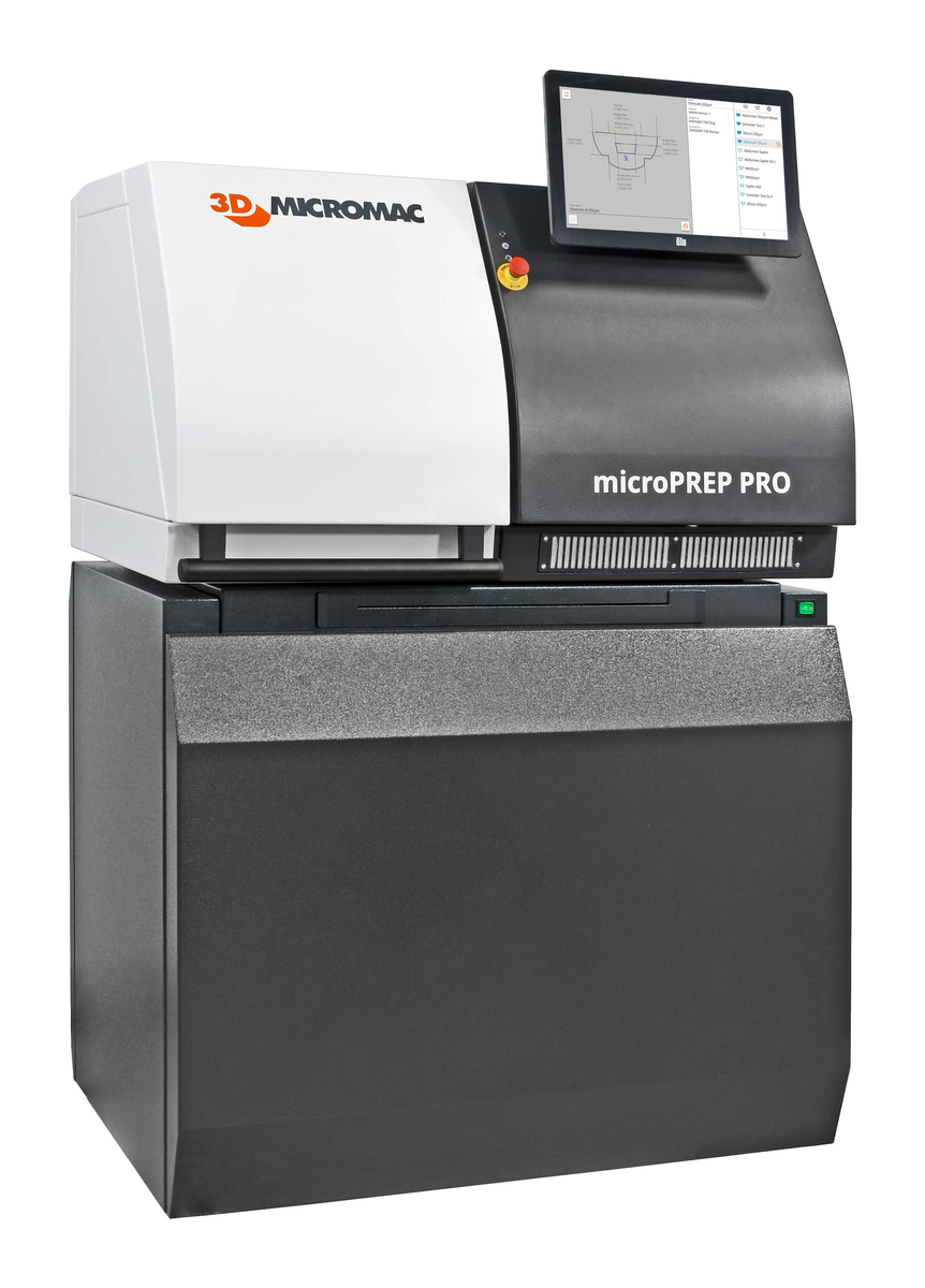
microPREP PRO Laser Sample Preparation System
-
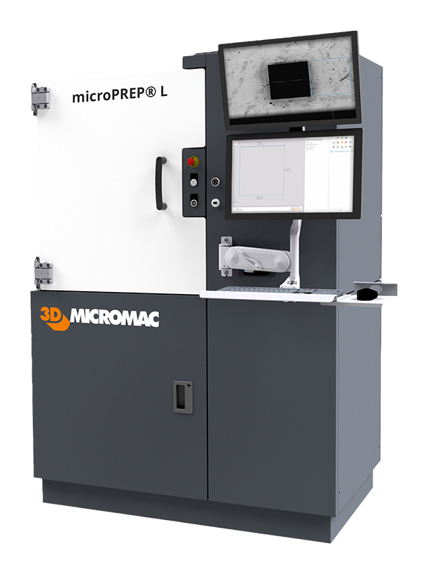
microPREP L Wafer- and Board-Level Laser Preparation System
Laser preparation directly on full 300 mm wafers and system-level boards, with multi-site runs and an optional sealed chamber, for failure analysis and QA.
-
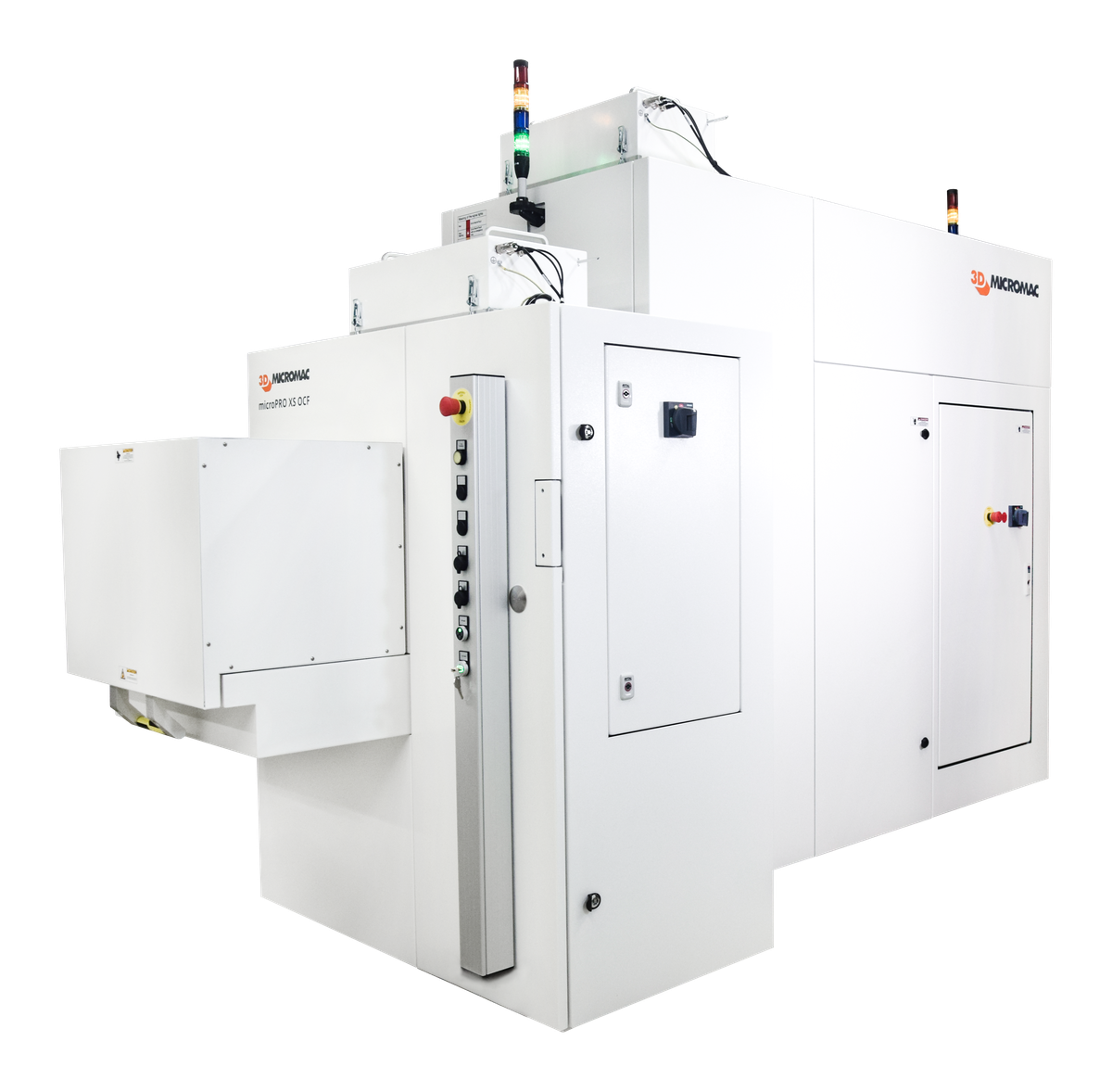
microPRO XS OCF Laser Annealing System for SiC Ohmic Contacts
UV laser annealing for backside ohmic contact formation on SiC power device wafers up to 200 mm, down to 40 µm thick.
-
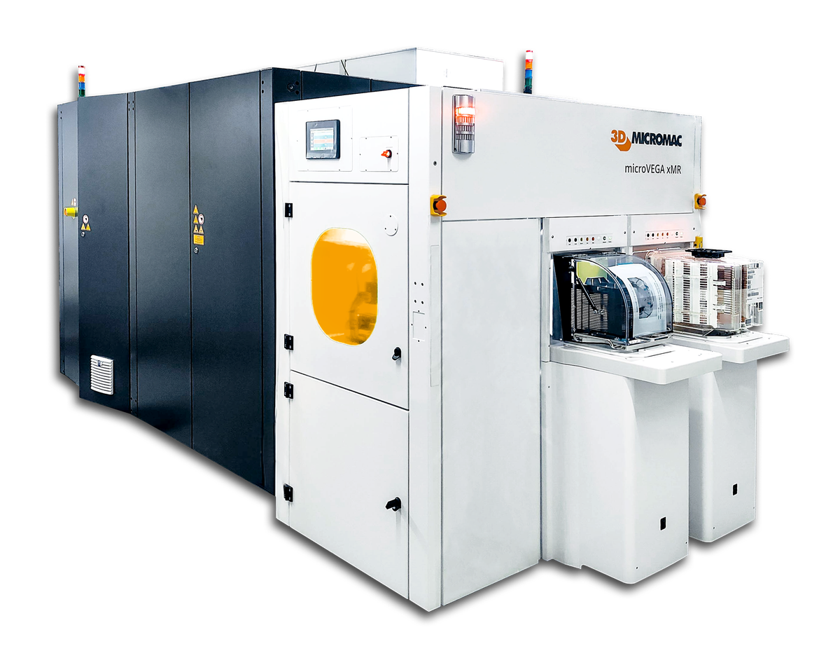
microVEGA xMR Selective Laser Annealing for Magnetic Sensors
Selective laser annealing with a local, rotatable magnetic field to programme GMR and TMR sensors on wafers up to 300 mm.
-
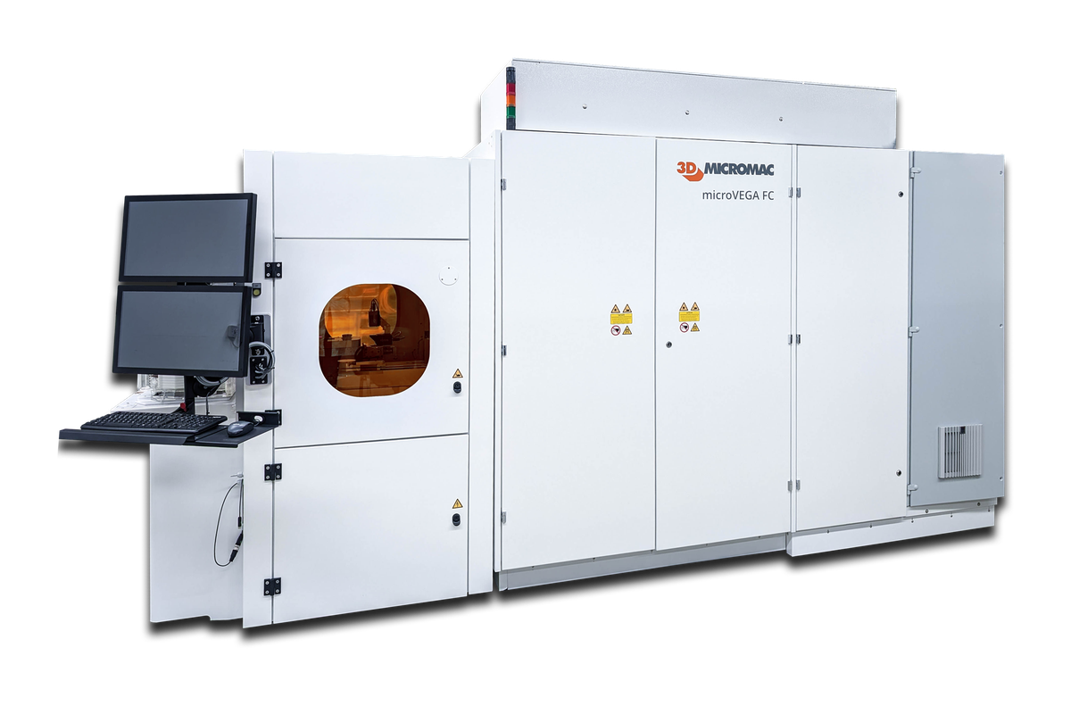
microVEGA FC Laser Trimming and Link Cutting System
Laser link cutting on 200 and 300 mm wafers for trimming, logic programming, and DRAM and microLED repair, at up to 400 mm/s.
-
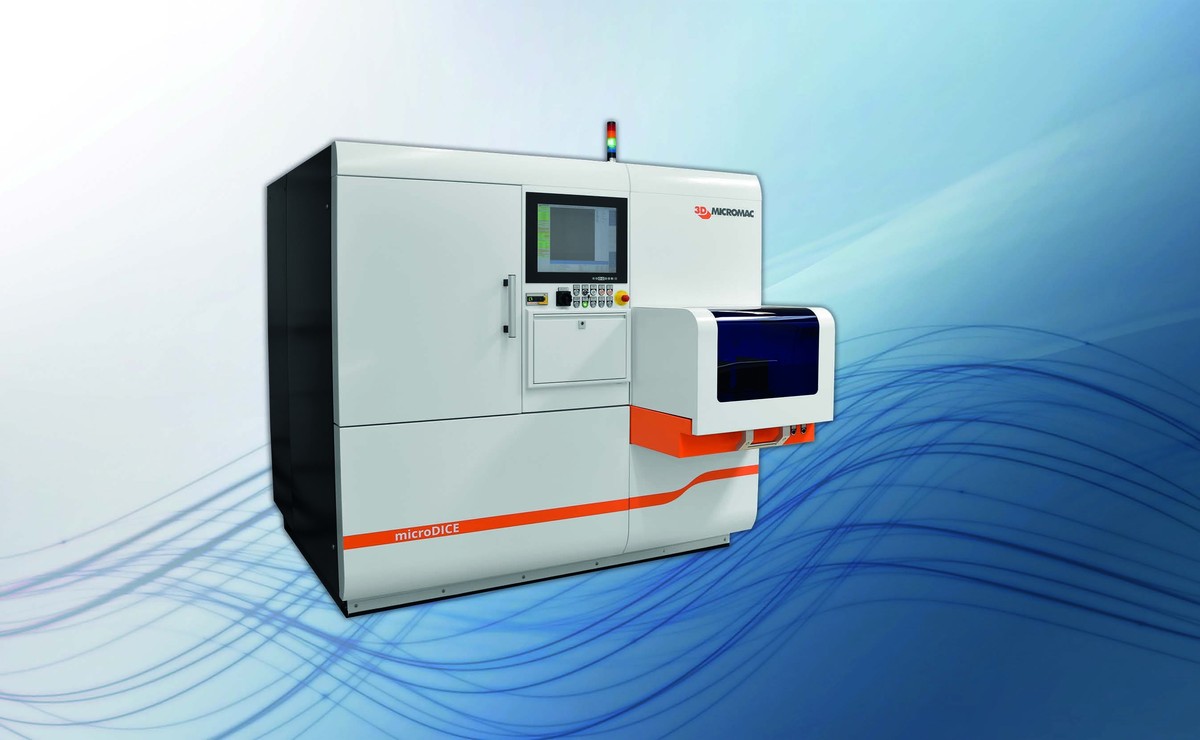
microDICE TLS-Dicing Laser Wafer Separation System
TLS-Dicing wafer separation for silicon, silicon carbide, germanium and gallium arsenide, up to 300 mm wafers at up to 300 mm/s.
-
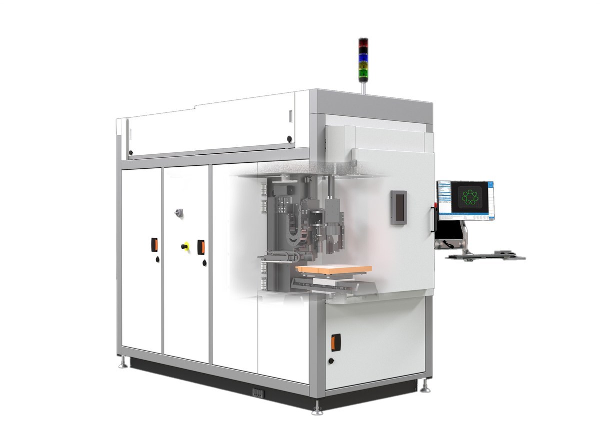
microPRO Industrial Laser Micromachining System
Configurable laser micromachining platform for cutting, drilling, engraving, structuring and laser lift-off, with ± 3 µm positioning on substrates up to 400 x 400 mm.
-
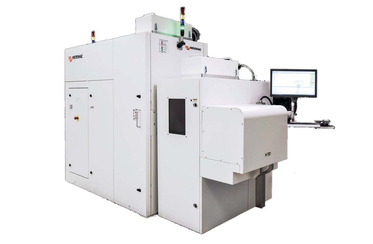
microPRO XS Compact Laser Micromachining System
Compact, configurable laser micromachining system for production, product development and applied research, on substrates up to 200 x 200 mm.