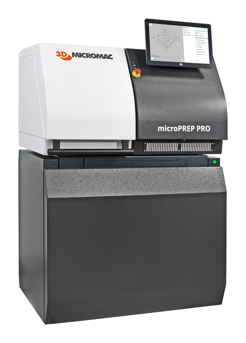
microPREP PRO Laser Sample Preparation System
microPREP PRO: laser sample preparation for TEM, FIB/SEM and atom probe
The 3D-Micromac microPREP PRO prepares specimens for electron microscopy, atom probe tomography, X-ray tomography and micromechanical testing by laser ablation. It takes coarse material removal off the focused ion beam, so the FIB only finishes what the laser has started. It’s the lab instrument in the microPREP family, used in semiconductor failure analysis and in research and development, and our sample preparation page covers the wider process.
Ultra-short pulses, minimal heat
Picosecond or femtosecond pulses keep heat influence at the surface to a few hundred nanometres or less. The laser ablates metals, semiconductors, ceramics, polymers and compound materials, and a choice of laser sources can be installed to suit the preparation work. Complex 3D-shaped samples are cut from generic patterns or DXF files.
What it prepares
For TEM it produces in-plane geometries and H-bars for cross-sections, leaving only the final polishing. Ahead of the FIB, the laser’s high ablation rate handles the box milling so FIB time drops to a minimum, and a slice-and-view geometry lets 3D analysis start directly in the FIB. Run as a lathe, it produces cylindrical samples at micrometre dimensions. Free-form shapes can be cut to almost any specification, with pre-defined shapes for bending and tensile test specimens.
microPREP PRO FEMTO
The FEMTO variant prepares atom probe probe cards with the size of each pillar specified individually, and a FIB step then gives each pillar its final shape. It won a Laser Focus World Innovators Award in 2024.
Handling and cleaning
microPREP PRO works with standard specimen stubs and mounts, so samples move on to the next process without rework. Overview and high-resolution process cameras and motorised stages position the work to micrometre precision. An optional CO2 Snow Jet removes debris in seconds without chemicals or cross-contamination.
Key features and benefits
- Laser preparation for TEM, FIB/SEM, atom probe, X-ray tomography and micromechanical testing
- Pico- or femtosecond pulses, with heat influence of a few hundred nanometres or less
- Choice of laser sources to suit the preparation task
- Complex 3D shapes from generic patterns or DXF files
- Standard specimen stubs and mounts
- Overview and high-resolution process cameras with motorised stages
- Optional CO2 Snow Jet cleaning
- A significantly shorter time-to-sample and a lower cost per sample, by 3D-Micromac’s account
To discuss your samples or arrange a trial at 3D-Micromac’s application laboratory in Chemnitz, contact us or request a quote.