Laser sample preparation for TEM, FIB/SEM, atom probe and micromechanical testing, using pico- or femtosecond sources and standard stubs and mounts.
Laser sample preparation for TEM, FIB/SEM and atom probe
Every specimen for an electron microscope or atom probe starts as a larger piece of material with a small region of interest inside it. Getting to that region is usually the slow part. Laser preparation removes the bulk quickly and precisely, and the focused ion beam then only has to finish the job. SiSTEM Technology supplies the 3D-Micromac microPREP range in the UK and Ireland, and sample preparation is one of the laser micromachining processes we support.
Where the time goes
A focused ion beam is precise and slow at removing material in volume. Using it for bulk removal ties up the instrument that much of a lab’s other work depends on. Mechanical routes such as sawing and grinding are quicker at the coarse stage, but they add damage and handling and struggle with complex geometries.
Laser preparation sits between the two. 3D-Micromac’s systems use ultra-short pulses in the picosecond or femtosecond range, which keeps heat influence at the surface to a few hundred nanometres or less. The laser can be positioned precisely and ablates metals, semiconductors, ceramics, polymers and compound materials. Complex 3D shapes are cut from generic patterns or DXF files. 3D-Micromac says the approach reduces time-to-sample significantly and lowers the cost per sample.
Techniques
TEM specimens
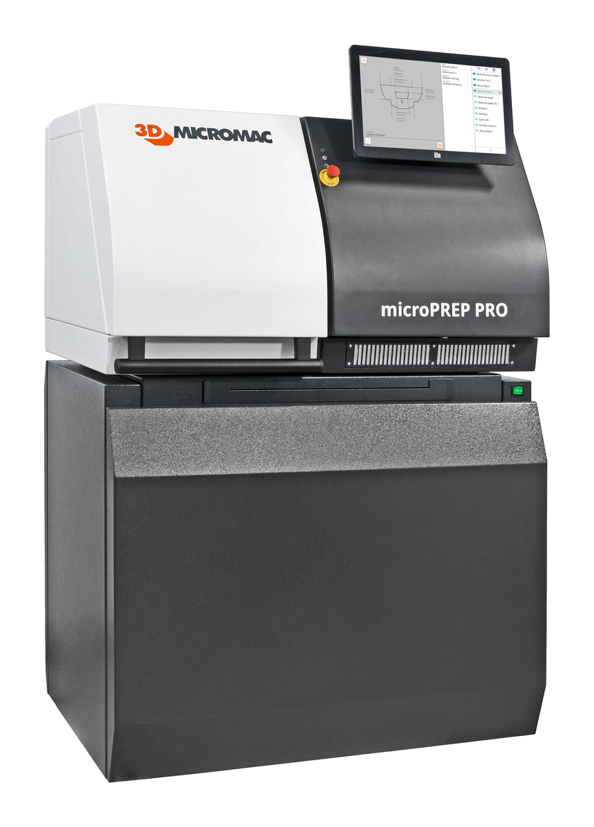
microPREP PRO produces geometries for in-plane TEM work and H-bars for cross-sections, leaving only the final polishing. One example in 3D-Micromac’s documentation is a chunk 3.2 mm long carrying several lamellas cut from an IC device, each 150 x 50 x 10 µm. Pre-thinned half-grid structures can also be cut from foils and thin sheet.
FIB/SEM cross-sections
The laser’s high ablation rate handles the box milling, and the FIB polishes only at the target position, which keeps FIB time to a minimum. microPREP PRO can also prepare a slice-and-view geometry so 3D analysis starts directly in the FIB.
Atom probe and 3D analysis
Run as a lathe, microPREP PRO produces cylindrical samples at micrometre dimensions. The PRO FEMTO variant prepares atom probe probe cards with the size of each pillar specified individually, and a FIB step then gives each pillar its final shape. PRO FEMTO won a Laser Focus World Innovators Award in 2024.
Micromechanical testing and free-form cutting
Samples can be cut to almost any shape a user specifies, with pre-defined shapes available for bending and tensile test specimens. 3D-Micromac’s examples include multi-pillar designs in steel alloy and micromechanical test samples in zirconium.
Wafer- and board-level preparation
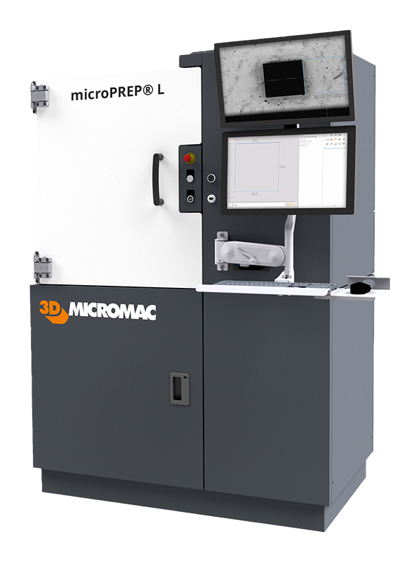
microPREP L takes the same approach to large substrates, from individual specimens up to full 300 mm wafers and system-level boards. Several sites can be prepared in one run, and a multi-axis system handles positioning, rotation and tilting without a dedicated setup for each task. A sealed process chamber is available for processing under vacuum, inert atmosphere or gas injection, and the system is prepared for automated semiconductor handling. Applications include device opening, delayering and cross-sections, and preparation for SEM, TEM, APT, X-ray tomography and nanoCT.
3D-Micromac also proposes microPREP L for targeted removal of defective structures. A faulty element on a wafer or board is identified and removed selectively, and the rest of the substrate carries on through production. They present it as an application idea rather than an established process, so it’s one to prove on your own material.
Laser and ion beam together
3D-Micromac positions microPREP as a complement to ion beam processing. One laser system can take over coarse preparation for several downstream tools, including FIB, BIB and plasma etching systems, so each of those spends its time on the specialist work it was bought for.
microPREP PRO or microPREP L?
microPREP PRO is the lab instrument. It works with standard specimen stubs and mounts, so samples move to the next step without rework. Overview and high-resolution process cameras guide the work, and an optional CO2 Snow Jet clears debris in seconds without chemicals or cross-contamination.
microPREP L suits failure analysis and quality assurance at wafer and board level, where regions of interest sit on large substrates and several need preparing at once. If you’re unsure which fits, send us a description of your samples and we’ll work it through with 3D-Micromac.
Try it on your own samples
3D-Micromac’s application laboratory in Chemnitz has access to SEM, FIB-SEM and TEM, so a preparation route can be tested and the result checked before anyone talks about a purchase order. We can arrange for your samples to go there.
Who should get in touch
Failure analysis labs, university electron microscopy and atom probe groups, materials and micromechanics research teams, and semiconductor teams in process development and quality assurance. We handle enquiries, quotations, applications support, installation and warranty in the UK and Ireland, and bring 3D-Micromac’s engineers in whenever the detail needs it.
Sample preparation systems
microPREP PRO
Laser sample preparation for TEM, FIB/SEM, atom probe, X-ray tomography and micromechanical testing.
microPREP PRO FEMTO
Femtosecond variant, preparing atom probe probe cards pillar by pillar.
microPREP L
Wafer- and board-level preparation on substrates up to 300 mm, with multi-site runs and an optional sealed chamber.
Contact us to discuss your samples or arrange a trial in Chemnitz.