

Laser sample preparation for TEM, FIB/SEM, atom probe and micromechanical testing, using pico- or femtosecond sources and standard stubs and mounts.
Laser micromachining for semiconductor, failure analysis and research
Laser micromachining removes or modifies material at micrometre scale with focused laser pulses. Nothing touches the workpiece, so tools don’t wear and a brittle wafer or delicate specimen sees no mechanical force. With the right pulse length and wavelength the heat stays close to where the work is done, which is why lasers now handle jobs on finished devices, thin wafers and samples bound for an electron microscope. SiSTEM Technology supplies laser micromachining systems from 3D-Micromac in the UK and Ireland.
When a laser is the right tool
Mechanical routes work well until the material gets hard and brittle or the part gets very thin. Silicon carbide is a good example: it’s hard enough that separating it with a blade is slow and costly. Specimen preparation is another. A TEM lamella cut mechanically carries damage that then has to be milled away, and a focused ion beam removing bulk material is an expensive way to spend instrument time.
Pulse length decides most of what happens next. Nanosecond sources heat material in a controlled way, which is what annealing needs. Picosecond and femtosecond pulses remove material so quickly that little heat spreads into the surrounding volume; on 3D-Micromac’s microPREP systems the heat-affected surface layer is a few hundred nanometres or less. Picking the source is the first process decision, and it’s one we’d make with you and 3D-Micromac’s applications engineers.
Processes we support
Sample preparation for TEM, FIB/SEM and atom probe
Ultra-short-pulse lasers take coarse material removal off the focused ion beam. The microPREP family prepares specimens for TEM, SEM cross-sections, atom probe tomography, X-ray tomography and micromechanical testing, across metals, semiconductors, ceramics, polymers and composites. 3D-Micromac quotes clean, precise structures within minutes, which leaves the FIB free for the final polishing it does best. The two methods work as one workflow. There’s more detail on our sample preparation page.
Laser annealing
Laser annealing heats a defined area so a contact or layer forms without heating the device around it. microPRO XS OCF forms ohmic contacts on the backside of SiC power device wafers up to 200 mm in diameter and down to 40 µm thick, with sheet resistance homogeneity below 1.1%. microVEGA xMR anneals selected sensor fields on GMR and TMR wafers inside a rotatable magnetic field, programming the reference layer with field orientation held to ± 0.01°. For whole-wafer furnace and rapid thermal work, see our thermal processing range.
Laser dicing
microDICE separates wafers into dies by TLS-Dicing, a thermal laser separation process that cleaves the wafer rather than cutting material away. It handles silicon, silicon carbide, germanium and gallium arsenide at up to 300 mm/s, on tape-and-frame wafers up to 300 mm. Narrower streets mean more dies per wafer, and the only process consumable is 600 ml of DI water per hour of active dicing. By 3D-Micromac’s own figures, that’s up to ten times the throughput of traditional dicing at up to 15 times lower cost of ownership, with zero kerf and edges free of micro-cracks.
Link trimming
microVEGA FC cuts metal links on finished chips to trim and calibrate analogue ICs and sensors. The same system handles DRAM and microLED repair. Spot diameter adjusts between 2 and 6 µm, and processing runs on the fly at up to 400 mm/s on wafers up to 300 mm.
Structuring, drilling and custom work
microPRO and microPRO XS are configurable platforms for cutting, drilling, engraving and structuring. Each is built around one laser source chosen from nanosecond, picosecond, femtosecond, fibre or CO2, and the larger microPRO takes substrates up to 400 x 400 mm. They suit metals, ceramics, glass and thin-film stacks. If a process doesn’t fit a standard machine, 3D-Micromac also designs custom systems.
Try it on your own material first
3D-Micromac’s application laboratory in Chemnitz runs picosecond, femtosecond, excimer, DPSS, CO2 and fibre sources, with SEM, FIB-SEM and TEM access for checking the result. We can arrange for your samples to be processed there before anyone talks about a purchase order. For limited lots or a ramp-up ahead of a tool purchase, 3D-Micromac also runs contract manufacturing in Chemnitz, so the machine investment can wait until your design is settled.
Who should get in touch
Failure analysis and microscopy labs, university research groups, SiC and GaN power device developers, magnetic sensor makers, and fabs looking at yield or throughput on one specific step. We handle enquiries, quotations, applications support, installation and warranty in the UK and Ireland, and bring 3D-Micromac’s engineers in whenever the detail needs it.
Send us the material and the result you need, and we’ll tell you quickly whether a laser process fits and which system to look at. If none of them does, we’ll say so.
Laser micromachining systems
microPREP PRO
Laser sample preparation for TEM, FIB/SEM, atom probe and micromechanical testing.
microPREP L
Large-area preparation on 300 mm wafers and system-level boards.
microPRO XS OCF
UV laser annealing for ohmic contacts on SiC and GaN.
microVEGA xMR
Selective laser annealing for GMR and TMR magnetic sensors.
microVEGA FC
Laser link trimming and memory repair.
microDICE
TLS-Dicing wafer separation for silicon, silicon carbide, germanium and gallium arsenide.
microPRO and microPRO XS
Configurable platforms for cutting, drilling and structuring.
Contact us to discuss an application, arrange a trial in Chemnitz, or ask for a quotation.
Laser Micromachining Products
-
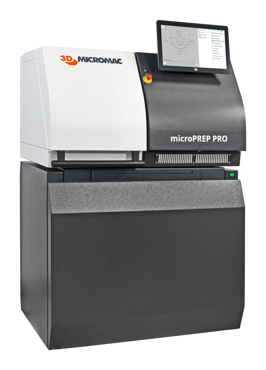
microPREP PRO Laser Sample Preparation System
-
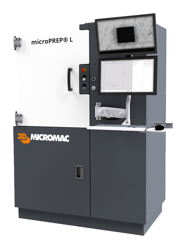
microPREP L Wafer- and Board-Level Laser Preparation System
Laser preparation directly on full 300 mm wafers and system-level boards, with multi-site runs and an optional sealed chamber, for failure analysis and QA.
-
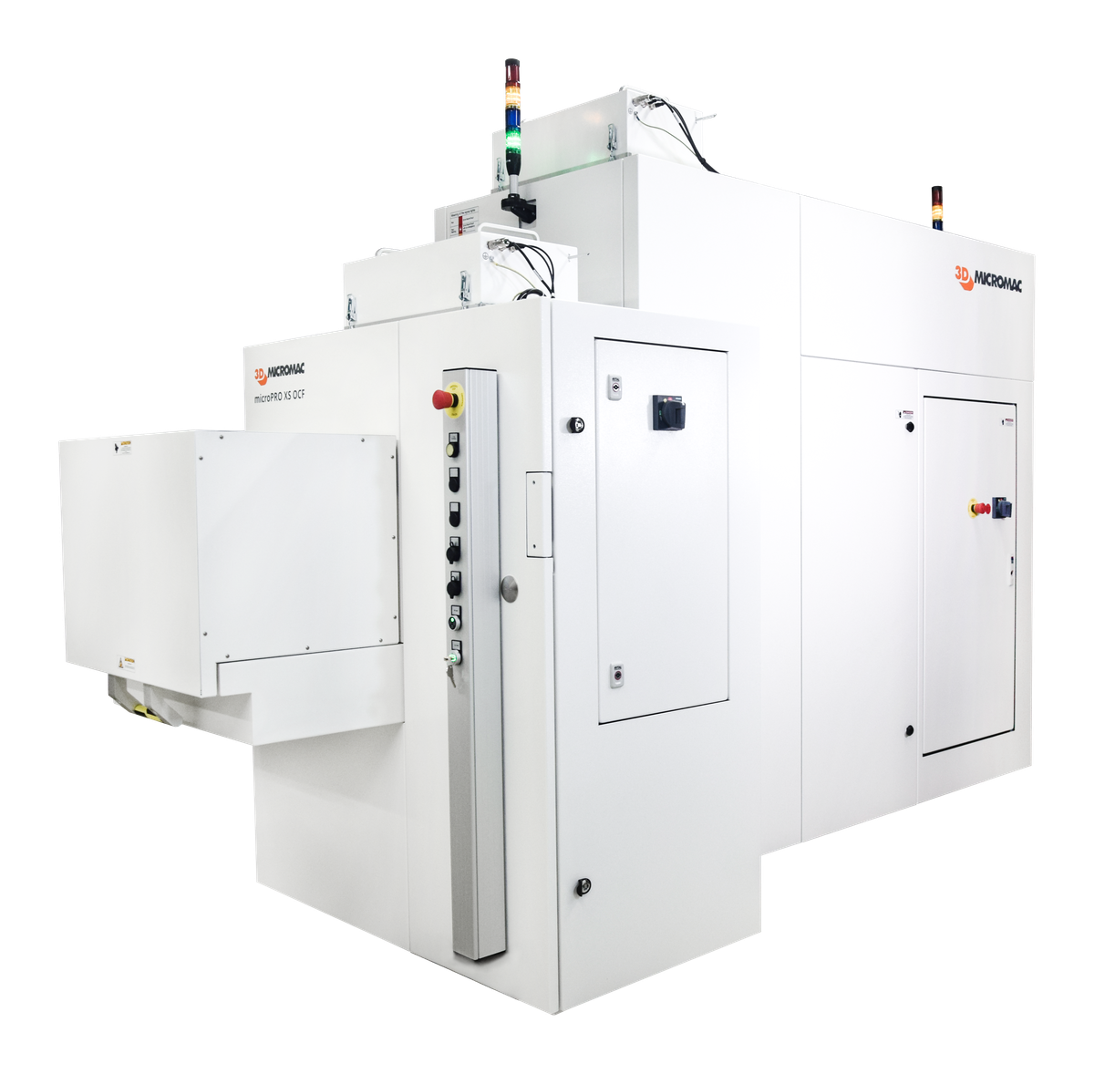
microPRO XS OCF Laser Annealing System for SiC Ohmic Contacts
UV laser annealing for backside ohmic contact formation on SiC power device wafers up to 200 mm, down to 40 µm thick.
-
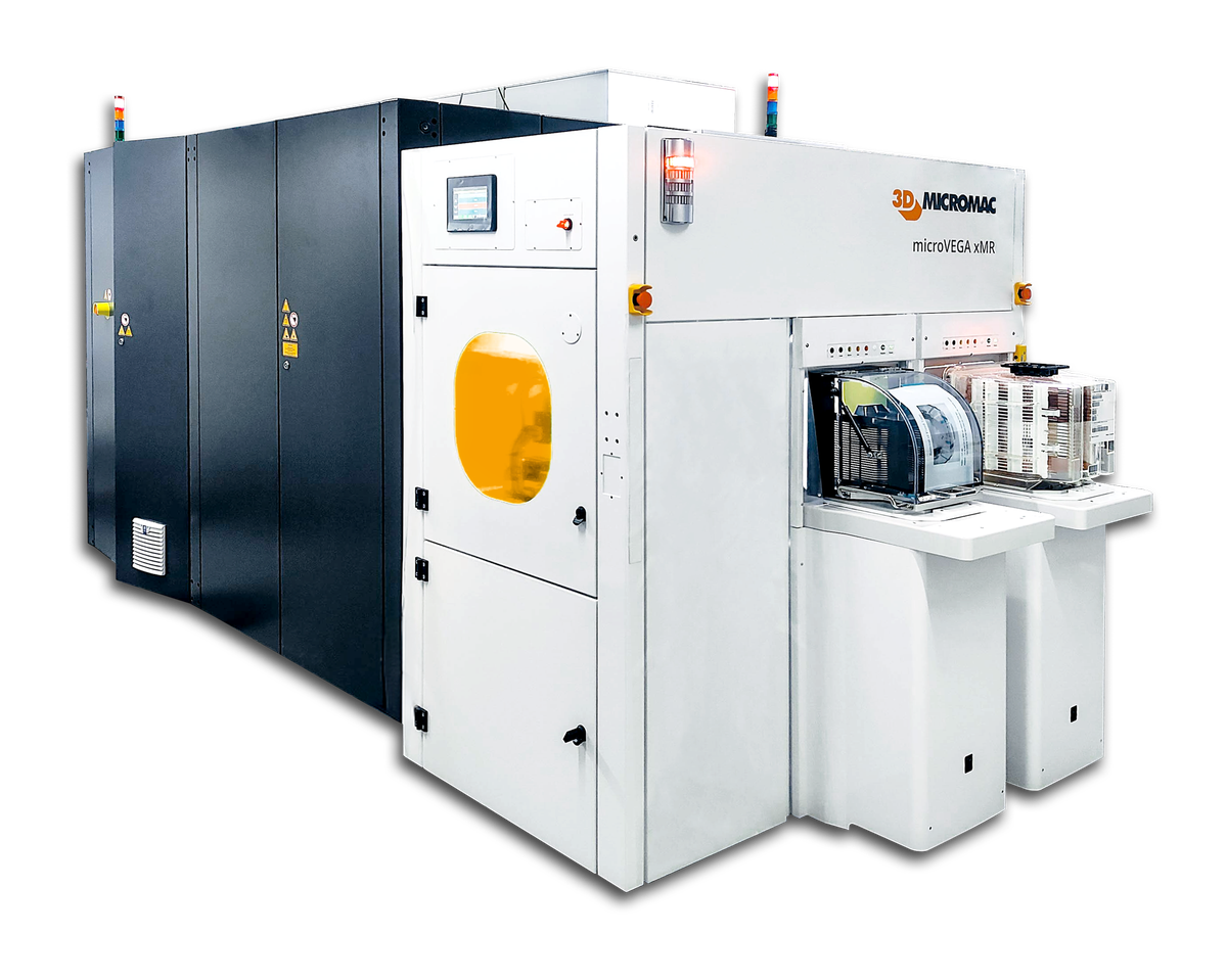
microVEGA xMR Selective Laser Annealing for Magnetic Sensors
Selective laser annealing with a local, rotatable magnetic field to programme GMR and TMR sensors on wafers up to 300 mm.
-
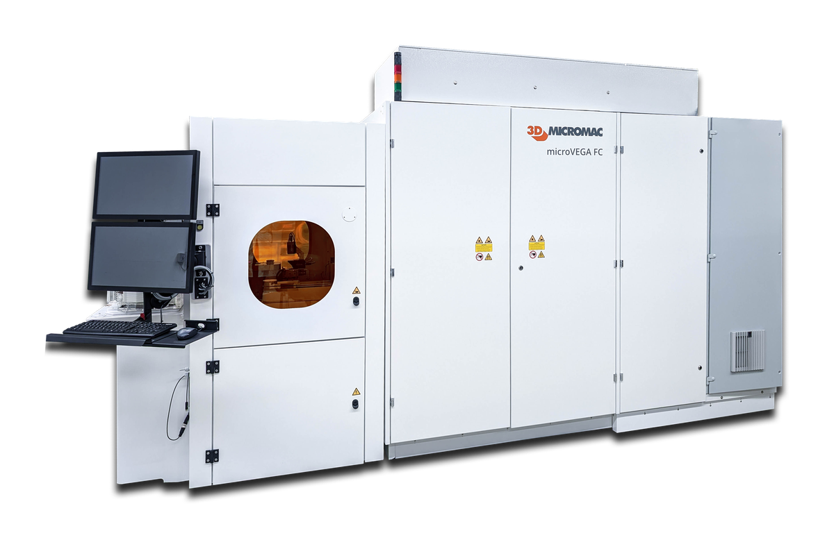
microVEGA FC Laser Trimming and Link Cutting System
Laser link cutting on 200 and 300 mm wafers for trimming, logic programming, and DRAM and microLED repair, at up to 400 mm/s.
-
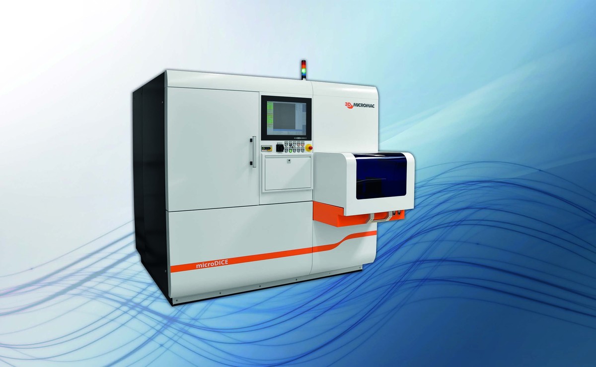
microDICE TLS-Dicing Laser Wafer Separation System
TLS-Dicing wafer separation for silicon, silicon carbide, germanium and gallium arsenide, up to 300 mm wafers at up to 300 mm/s.
-
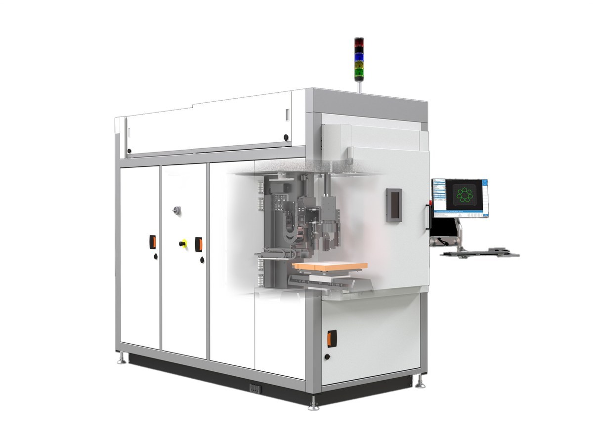
microPRO Industrial Laser Micromachining System
Configurable laser micromachining platform for cutting, drilling, engraving, structuring and laser lift-off, with ± 3 µm positioning on substrates up to 400 x 400 mm.
-
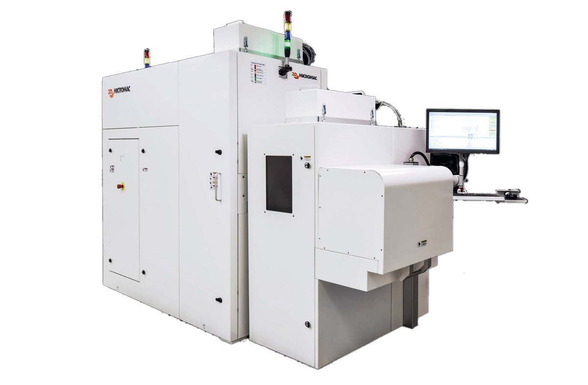
microPRO XS Compact Laser Micromachining System
Compact, configurable laser micromachining system for production, product development and applied research, on substrates up to 200 x 200 mm.