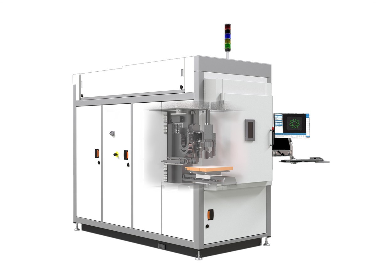
microPRO Industrial Laser Micromachining System
microPRO: a configurable laser micromachining platform for production
The 3D-Micromac microPRO is an adaptable laser micromachining system used mainly in industrial production. It’s built around one laser source and a set of configuration packages, so the same platform can be set up for cutting, drilling, engraving, structuring or laser lift-off. It works on metals, alloys, transparent and biological substrates, ceramics and thin-film compound systems. It’s one of the laser micromachining processes we support for semiconductor and research and development customers, and the smaller microPRO XS covers the same ground in a compact format.
Configuration packages
Packages include high-speed cutting, drilling, engraving, structuring and modification, laser lift-off, cylindrical machining and customised solutions. The laser source is chosen to suit the work, from nanosecond, fibre, femtosecond, picosecond or CO2, and delivered through 2D or 3D galvo scanners or fixed optics, with power measured at workpiece level.
Precision and working area
A direct-driven XY positioning system gives 600 x 500 mm of travel, with positioning accuracy of ± 3 µm and repeatability of ± 1 µm. Substrates up to 400 x 400 mm fit the working area, and larger sizes are available on request. Z positioning is automatic, and workpiece alignment can be manual, semi-automated or fully automated using the XY system and optical measurement.
Handling and software
Automatic handling for wafers, cassettes and trays is available, with loading and unloading built to your specification and RFID or Data Matrix reading. The workpiece clamping unit changes quickly. microMMI software controls every hardware component and machining parameter, with separate user levels, and takes DXF, CSV, Gerber, CLI and GDSII files. The system sits in a laser class 1 housing with an integrated control panel and includes active exhaust.
Key features and benefits
- One laser source chosen from ns, fibre, fs, ps or CO2
- Configuration packages for cutting, drilling, engraving, structuring, laser lift-off and cylindrical machining
- 2D or 3D galvo scanners or fixed optics
- 600 x 500 mm travel, ± 3 µm positioning accuracy, ± 1 µm repeatability
- Substrates up to 400 x 400 mm, larger on request
- Optional automatic handling for wafers, cassettes and trays
- microMMI software with DXF, CSV, Gerber, CLI and GDSII input
- 3,010 x 1,490 x 2,270 mm, approx. 4 t
To discuss your process or arrange trials at 3D-Micromac’s application laboratory in Chemnitz, contact us or request a quote.