microVEGA xMR Selective Laser Annealing for Magnetic Sensors
microVEGA xMR: selective laser annealing for GMR and TMR magnetic sensors
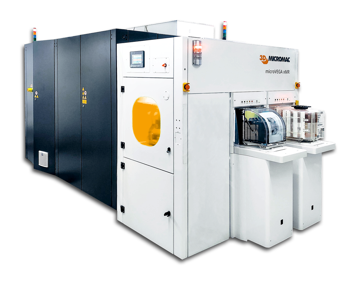
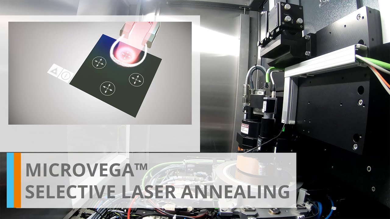
The 3D-Micromac microVEGA xMR programmes the reference layer of GMR and TMR magnetic sensors on the wafer. A selective laser spot heats defined sensor fields while a local, rotatable magnetic field sets their orientation, so fields can be programmed individually across a single wafer. 3D-Micromac says the approach reduces process steps and simplifies production of integrated monolithic sensor packages. It’s one of the laser micromachining processes we support for semiconductor sensor manufacturing.
Precise, local heating
Magnetic field orientation is held to ± 0.01°. The heat-affected zone reaches only a few micrometres beyond the sensor chip, so sensors can sit closer together and closer to the logic they feed. A nanosecond NIR source with the spot size in X and Y programmable by recipe does the heating, and energy is logged by a power sensor at chuck level, a beam analyser at wafer level and an integrated gauss-meter.
One platform for GMR and TMR
GMR and TMR sensors run on the same platform, with in-plane and out-of-plane programming, on wafers up to 300 mm. Recipes cover pulse energy, sensor dimensions, spacing, orientation and magnetic flux, and no consumables or product-specific parts are required. microVEGA xMR won a Laser Focus World Innovators Award in 2022.
Options and standards
Options include a heating chuck, a second laser source for other wavelengths and pulse lengths, EFEM handling for SMIF, FOUP and open cassette, automatic magnet exchange and SECS/GEM. The system is laser class 1 and ISO class 5, with CE, UL and SEMI available as options.
Key features and benefits
- Selective laser annealing for GMR and TMR sensors on one platform
- In-plane and out-of-plane programming
- Magnetic field orientation ± 0.01°
- Heat-affected zone only a few micrometres beyond the sensor chip
- Wafers up to 300 mm, bridge-tool capability optional
- In-situ energy and field measurement, all logged
- No consumables or product-specific parts
To discuss your sensor process or arrange trials in Chemnitz, contact us or request a quote.