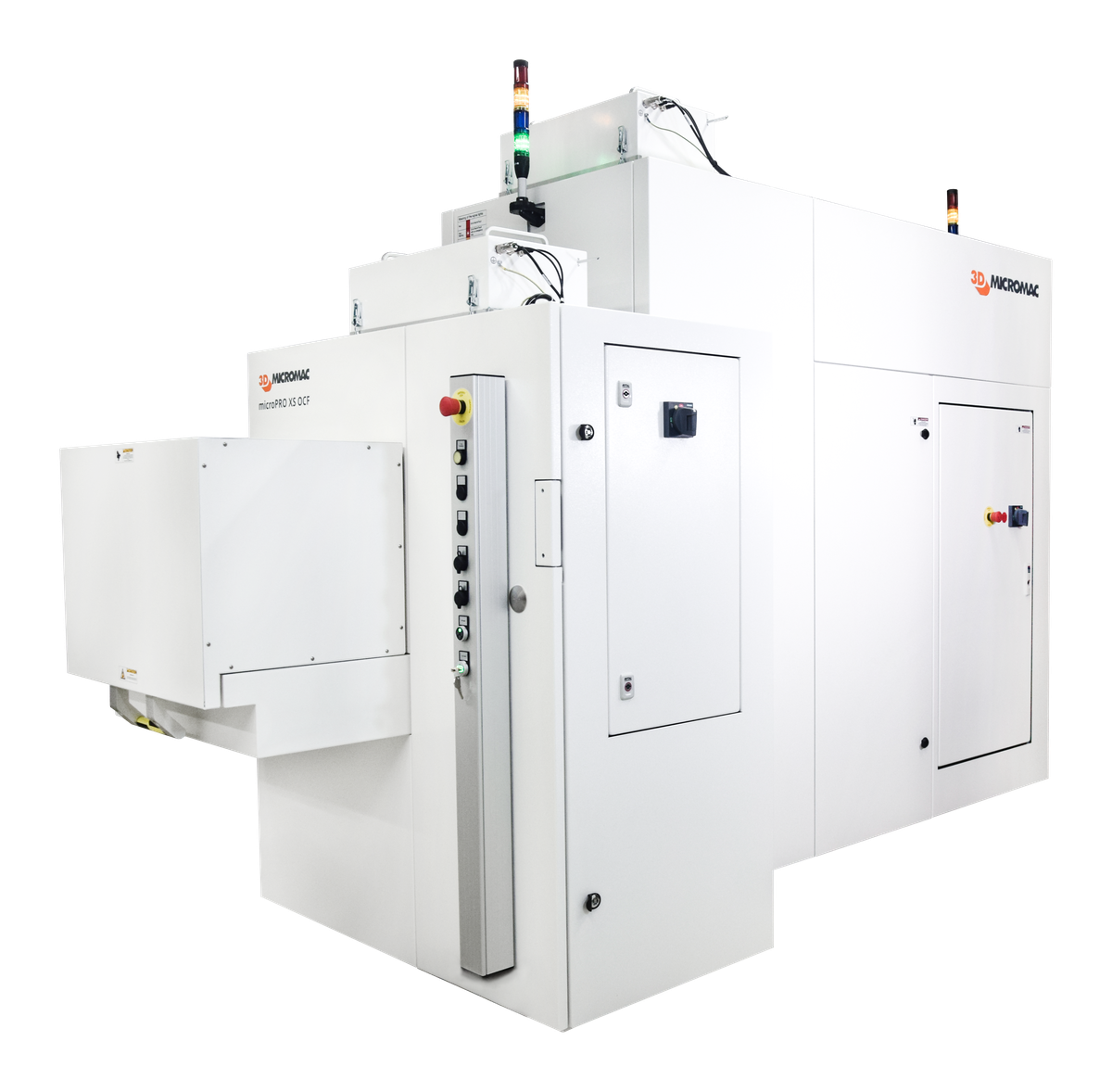
microPRO XS OCF Laser Annealing System for SiC Ohmic Contacts
microPRO XS OCF: laser annealing for ohmic contacts on SiC power devices
The 3D-Micromac microPRO XS OCF forms ohmic contacts on the metallised backside of silicon carbide power device wafers by UV laser annealing. Heating is confined to the backside contact layer, which 3D-Micromac says minimises thermal effects on device performance. It’s one of the laser micromachining processes we support for semiconductor manufacturing, alongside our thermal processing range for whole-wafer work.
The process
A nanosecond UV DPSS laser with galvo scanning and an adjustable spot profile anneals the backside metal. Recipe control sets the NixSiy phase and thickness, with fluence at wafer level between 0.5 and 6 J/cm². Processing runs in a recipe-controlled chamber under nitrogen or air, with oxygen concentration monitored. 3D-Micromac notes the process also cures grinding defects.
Throughput and uniformity
The system anneals up to 22 wafers an hour on 6″, with sheet resistance homogeneity δ below 1.1%. 6″ and 8″ wafers are processed without stitching, so no tool adaptation is needed between sizes. It handles SiC, GaN and other compound wafers down to 40 µm thick, with ultra-thin wafer handling available and capability for wafers on a glass carrier.
Built for production
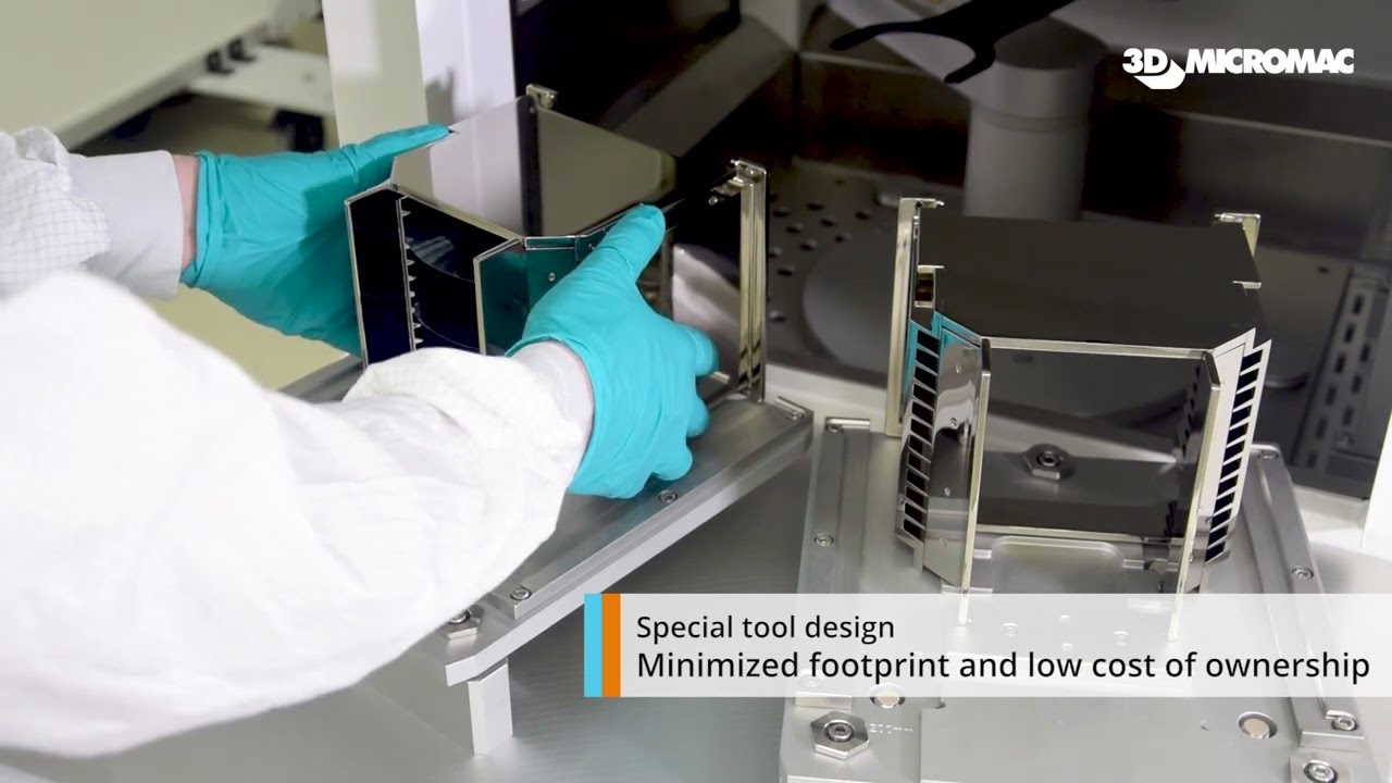
Handling is fully automated, from open cassette or SMIF pods, with an ID reader and automatic alignment. The system is SEMI compatible, CE, UL and KC marked and laser class 1, with SECS/GEM available on request. 3D-Micromac describes the process as proven in semiconductor mass production.
Key features and benefits
- Ohmic contact formation on the backside of SiC power device wafers
- Up to 22 wafers an hour on 6″
- Sheet resistance homogeneity δ < 1.1%
- 6″ and 8″ without stitching, wafers down to 40 µm
- Nanosecond UV DPSS laser, fluence 0.5 to 6 J/cm²
- Recipe-controlled chamber, nitrogen or air, O2 monitoring
- Open cassette or SMIF handling, SECS/GEM on request
- Footprint 1,340 x 3,165 mm including handling
To discuss your SiC process or arrange trials in Chemnitz, contact us or request a quote.