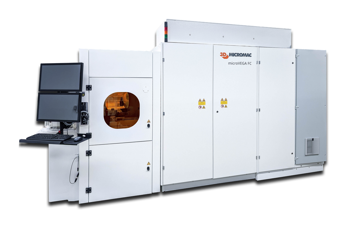
microVEGA FC Laser Trimming and Link Cutting System
microVEGA FC: laser trimming and link cutting on semiconductor chips
The 3D-Micromac microVEGA FC cuts metal links on chips at wafer level to enable or disable specific functions. It trims potentiometers and programmes digital logic circuits, and it’s also suited to DRAM memory repair, microLED repair and implementing security functions. Calibrating analogue ICs and sensors this way compensates for variation in the manufacturing process, which 3D-Micromac links to higher yield and more consistent performance. It’s one of the laser micromachining processes we support for semiconductor manufacturing.
How it works
A laser spot a few micrometres across moves continuously over the wafer and processes defined structures on multiple dies on the fly, at up to 400 mm/s. The structures are around 1 to 2 µm, so the spot has to be placed very precisely in three dimensions. System positioning accuracy is ± 200 nm at 3 sigma, and the process environment is held at 21 °C ± 0.1 K.
Laser and process control
The standard source is a nanosecond laser at 1,062 nm, with 532 nm and 355 nm available and a configurable pulse shape and length. Spot diameter adjusts freely from 2 to 6 µm. An integrated online energy sensor, laser beam analyser and in-situ camera give 100 percent process control, and all relevant data are logged.
Production handling
A bridge tool takes both 200 mm and 300 mm wafers. Handling options include automatic wafer handling with FOUP, SMIF or open cassette load ports, manual, MGV or AGV loading, a prealigner, RFID and wafer ID readers, and SECS/GEM. The system is laser class 1 and ISO class 3, built to SEMI S2/S8, with CE or UL as an option.
Key features and benefits
- Laser link cutting for trimming, logic programming and memory repair
- On-the-fly processing at up to 400 mm/s
- System positioning accuracy ± 200 nm (3 sigma)
- Spot diameter adjustable from 2 to 6 µm
- 1,062 nm standard wavelength, with 532 nm and 355 nm available
- Integrated energy sensor, beam analyser and in-situ camera, with all data logged
- 200 mm and 300 mm wafers on one bridge tool
- 1,643 x 2,540 x 4,134 mm including automatic wafer handling
To discuss your trimming or repair process, contact us or request a quote.