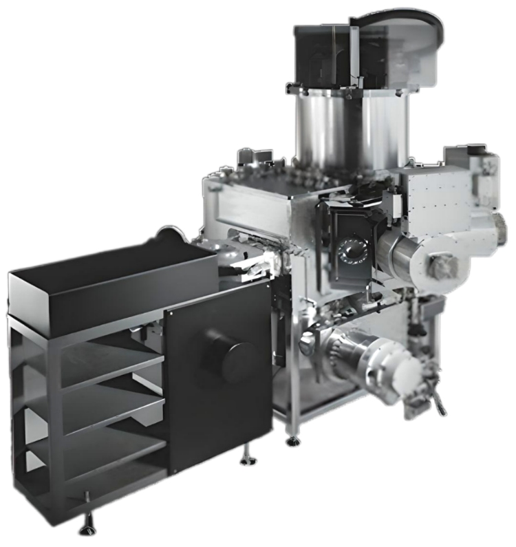
- Versatile Deposition Capabilities
- Multi-Target Carousel
- Precision Substrate Handling
- Empowering Ion Assist Capability
- Compact Design, Premium Results
Email: info@sistemtechnology.com Call: +44 (0)1327 362 844
In the realm of thin film deposition techniques, where precision and control reign supreme, Ion Beam Sputtering (IBS) stands tall as a pinnacle of excellence. As a form of Physical Vapour Deposition (PVD), IBS boasts unparalleled advantages, offering a realm of possibilities across various industries such as optics, sensors (MEMS), thin film solar cells, and semiconductors.
Ion Beam Sputtering, also known as Ion Beam Deposition (IBD) or Ion Beam Sputter Deposition (IBSD), represents a sophisticated method for crafting high-quality thin films spanning an array of materials, from metals to semiconductors and dielectrics. Its widespread adoption within the optics industry underscores its efficacy in producing dense, uniform layers—a fundamental requirement for optimal performance in optical applications.
At its core, Ion Beam Sputtering operates on a simple yet powerful principle. A broad beam of collimated ions is directed towards a target material, inducing the ejection of target atoms or molecules. These liberated particles, propelled with high kinetic energy, condense onto a substrate, forming meticulously crafted thin layers devoid of pinholes.
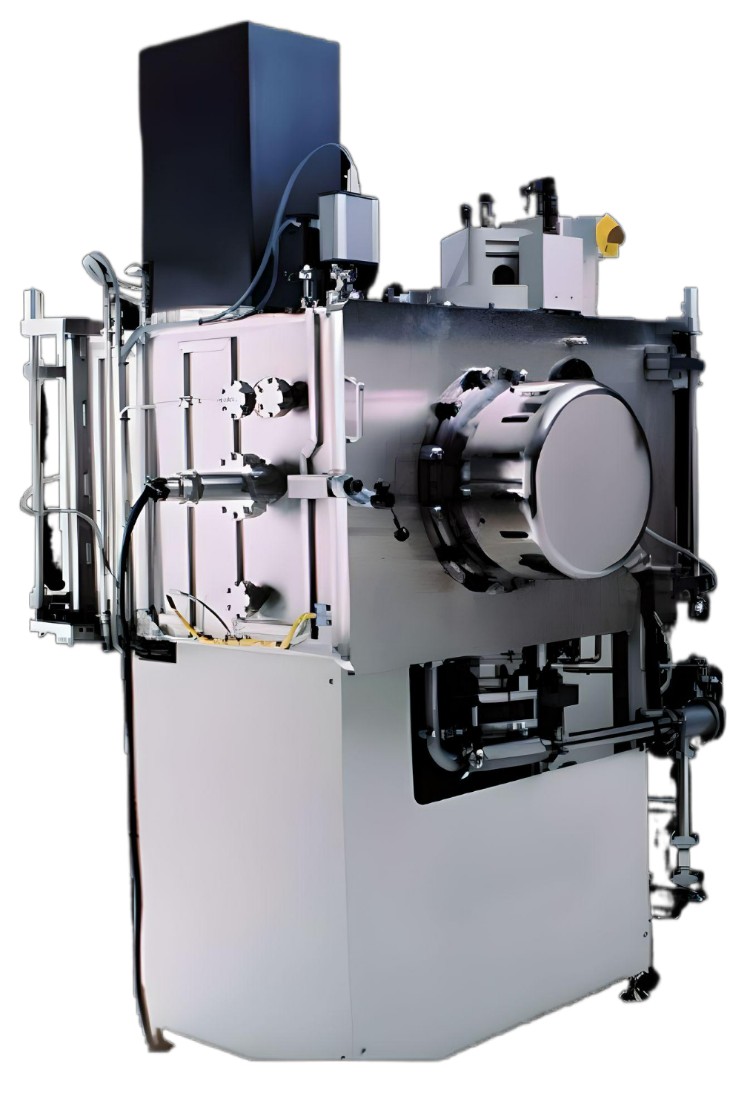
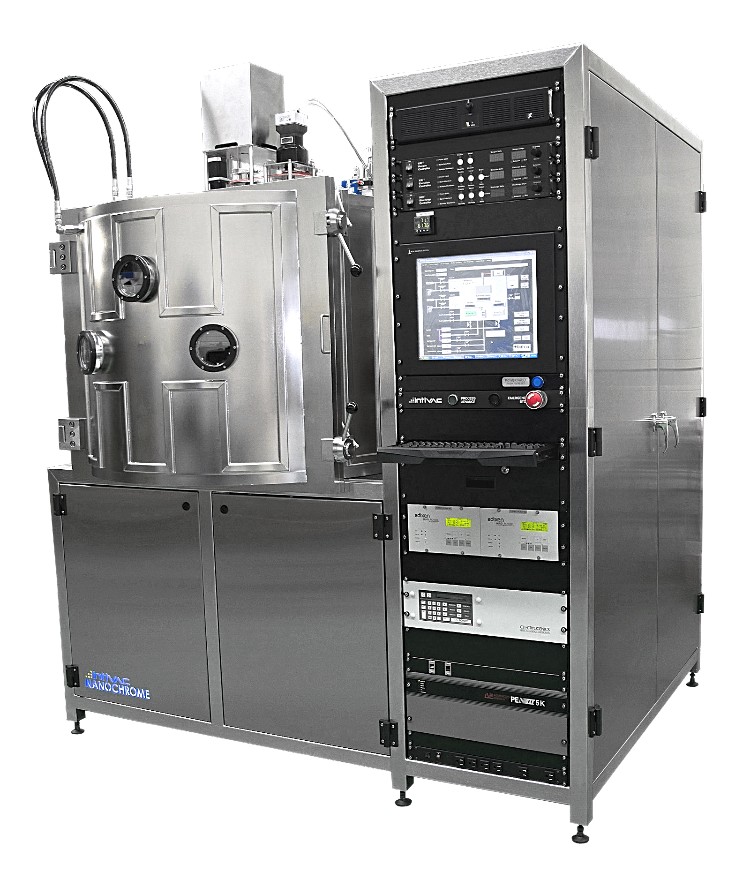
SiSTEM Technology is very proud to distribute Intlvac Thin Film Ion Beam Sputtering Deposition tools throughout Europe, and these include the entry level Nanoquest I, the combo (sputter & etch) Nanoquest I, 150mm Nanoquest II, 200mm batch tool – Nanoquest III, and the 250mm sputter up Nanochrome IV.
At the heart of the process lies the ion source, where high voltage energises inert gas atoms, typically Argon (Ar), transforming them into a stream of positively charged ions. These ions, accelerated towards the target, carry the energy necessary for efficient sputtering.
Serving as the focal point of ion bombardment, the target material relinquishes its atoms or molecules under the relentless assault of energetic ions. This process is fundamental to the generation of thin films with exceptional properties.
Positioned strategically within the chamber, the substrate holder provides a stable platform for the deposition process. Here, the liberated particles from the target material coalesce into precise thin films, ready to fulfill their intended purpose.
With meticulous control over deposition parameters and ion energy, IBS facilitates the creation of thin films with unparalleled precision, essential for demanding applications in optics and semiconductor industries.
The low chamber pressure and high-energy ions characteristic of IBS ensure uniformity across deposited layers, mitigating inconsistencies often encountered in alternative deposition techniques.
Unlike its counterparts, IBS offers strict control over layer stoichiometry, minimising impurities and ensuring the desired composition of thin films—a crucial factor in achieving optimal performance in various applications.
From metals to insulators, magnetic materials to refractory metals, IBS accommodates an extensive range of materials, providing versatility and flexibility to suit diverse industry needs.
In the pursuit of pristine optical surfaces and coatings, IBS reigns supreme, offering the precision and uniformity necessary for cutting-edge optical devices and systems.
From microelectromechanical systems (MEMS) to sensor arrays, the precision afforded by Ion Beam Sputter Deposition enables the creation of intricate, high-performance sensor components crucial for a myriad of applications.
In the realm of renewable energy, the efficiency and reliability of thin film solar cells hinge upon the quality of their coatings. IBS delivers the uniformity and stability required to maximise energy conversion efficiency.
As semiconductor devices push the boundaries of performance, the demand for precise thin film deposition methods escalates. Ion Beam Sputter Deposition meets this demand head-on, offering the control and reproducibility essential for semiconductor fabrication.
In the realm of thin film deposition techniques, Ion Beam Sputtering emerges as a beacon of precision, offering unparalleled control and versatility across a myriad of industries. From optics to semiconductors, the impact of Ion Beam Sputter Deposition reverberates, unlocking new frontiers of possibility and innovation. With its unmatched precision and steadfast reliability, Ion Beam Sputtering stands poised to shape the future of thin film technology, driving progress and innovation across diverse fields of endeavour.
Contact us today to find out how we can assist your project with our expertise.
Get a quote quickly by clicking the link and submitting your requirements via our quote request page.
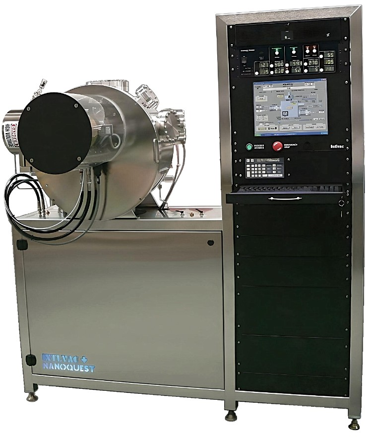
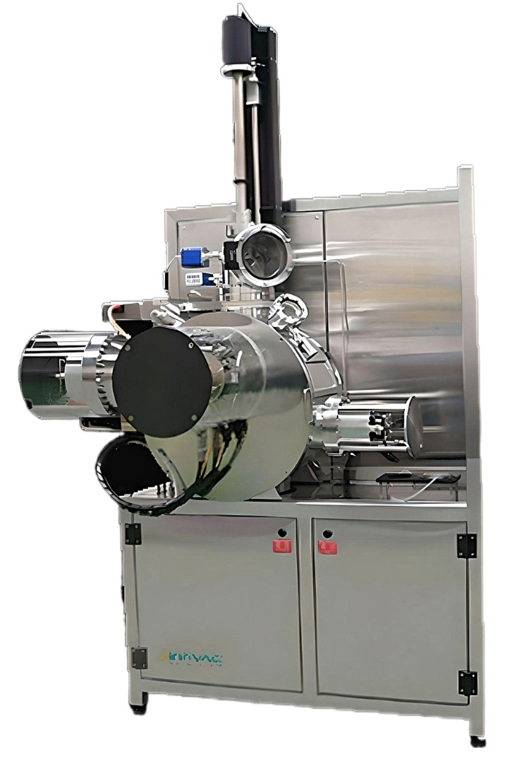
Superior PVD Deposition Capability
Large Multi-Target Carousel
Rotating and Angle-Tilt Substrate Stage
Ion Assist Capability and Monitoring
High-Density Coatings with Low Particle Levels