

- Indium bump deposition on wafers up to 200 mm
- Full 4 µm indium run in under 2.5 hours
- Automatic or manual load lock with in-situ pre-clean
- Wafer temperature control from +60°C to -75°C
- Hundreds of depositions without opening the main chamber
Thin Film Deposition Systems
Thin film deposition puts down layers of material, from a few nanometres to several microns thick, onto wafers, optics and components. The method you choose decides the film’s density, purity, stress and uniformity, and how well it suits lift-off, optical multilayers or production volumes. Intlvac Thin Film builds systems for each of the main physical vapour deposition (PVD) methods, and for diamond-like carbon by PECVD. SiSTEM is Intlvac’s partner for the UK, Ireland and most of Europe.
Electron beam evaporation
An electron beam heats source material in a water-cooled crucible until it evaporates, and the vapour condenses on the substrate. The deposition front is directional, which suits lift-off, and a multi-pocket gun lets one run build metal and dielectric multilayers. Ion assist densifies the film as it grows.
- The Nanochrome I is an R&D and pilot system with a 4- or 6-pocket e-beam gun.
- The evaporation version of the Nanochrome II adds thermal sources and substrate heating options up to 800°C.
- The Nanochrome Pico is the compact R&D option.
More on choosing one: electron beam evaporation systems.
Magnetron sputtering
A magnetron holds a plasma close to the target, and ions from it sputter target atoms onto the substrate. Sputtering suits metals, alloys and reactive oxide and nitride films, and gives good adhesion and step coverage.
- The sputter version of the Nanochrome II runs several cathodes from pulsed DC supplies, with in-situ stress monitoring.
- The Nanochrome Pico takes up to three 3″ magnetrons, set up to sputter up or down.
Ion beam sputter deposition
A broad ion beam from a separate source sputters the target, so the process runs at low pressure, away from the plasma. The films are dense and smooth, with low particle counts, which suits precision optical coatings. The Nanochrome IV IBSD coats substrates up to 250 mm. There’s more on the method on our ion beam sputter deposition page.
Diamond-like carbon by PECVD
The Aegis deposits diamond-like carbon from hydrocarbon precursors at low temperature. It’s used for protective and anti-reflection coatings on IR optics, and as a hard mask for lithium niobate etching. More on the DLC coating systems page.
Indium evaporation for bump bonding
The Icarus evaporates indium for bump bonding on wafers up to 200 mm, for focal plane arrays, quantum devices and semiconductor packaging. More on the process: indium bump deposition.
Etch on the same platform
Several Intlvac deposition systems also etch. The Nanochrome I can run e-beam evaporation, magnetron sputtering and ion beam etching in one pump-down, and the Nanoquest I IBSD Combo deposits and etches on substrates up to 100 mm. For etch on its own, see ion beam etching and milling.
Scoping a deposition system
To put a system together with Intlvac, we’ll ask about:
- the films you need and the materials in each layer
- thickness, uniformity and stress targets
- substrate size, shape and how many per run
- R&D, pilot or production use, and whether a load lock is needed
- substrate heating or cooling, and how you need to monitor the process
Working with SiSTEM
SiSTEM is Intlvac’s partner for the UK, Ireland and most of Europe. We scope your system with you and Intlvac’s engineers, and stay your local contact through quotation, installation and after-sales.
Thin Film Deposition Products
-
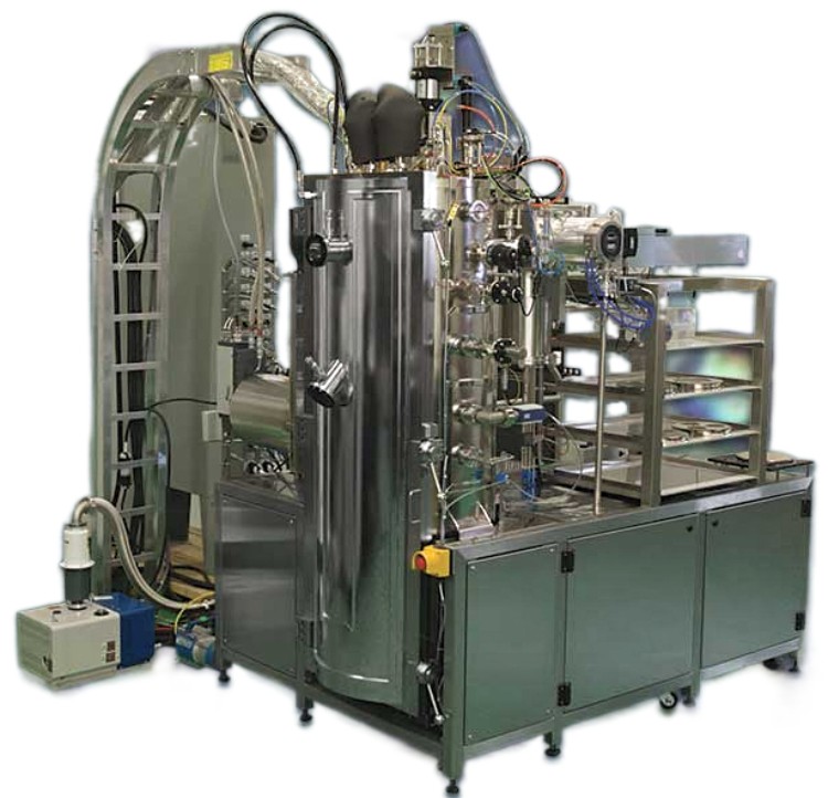
Icarus Indium Deposition System
-
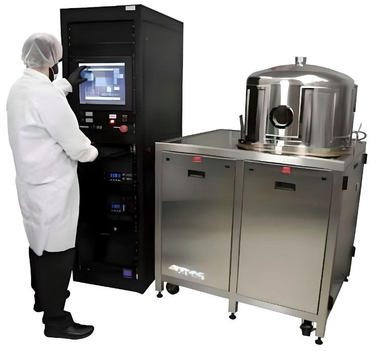
Aegis Diamond-Like Carbon Deposition
- Low-temperature PECVD diamond-like carbon
- Single-layer AR and protective coating for IR optics
- Better than ±1% Tavg uniformity over 508 mm
- Qualified to MIL-C-48497A, TS1888 and ISO 9022
- DLC hard masks for lithium niobate etching
-
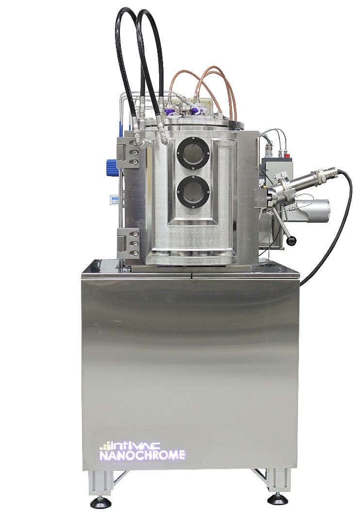
Nanochrome Pico Thin Film Deposition
- Compact R&D PVD in a 16″ D-shaped chamber
- Sputter up or sputter down, easily reconfigured
- Magnetron, e-beam, thermal and Knudsen cell sources
- Optional heated stage to 800°C
- Load lock between a pair of Pico chambers
-
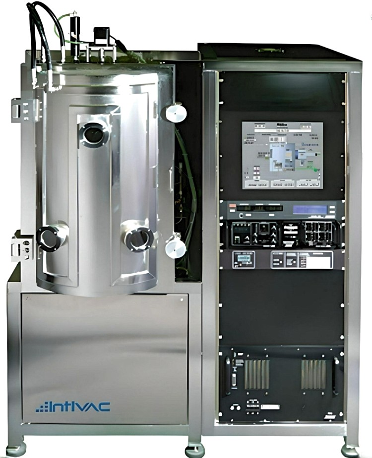
Nanochrome I Thin Film Deposition
- R&D and pilot PVD with a 4- or 6-pocket e-beam gun
- E-beam, sputtering and ion beam etching in one pump-down
- Water-cooled stage with automatic angle control
- 5×10⁻⁶ Torr in under 15 minutes, 5×10⁻⁸ Torr ultimate
- AUTOSYS control with recipe and run logging
-
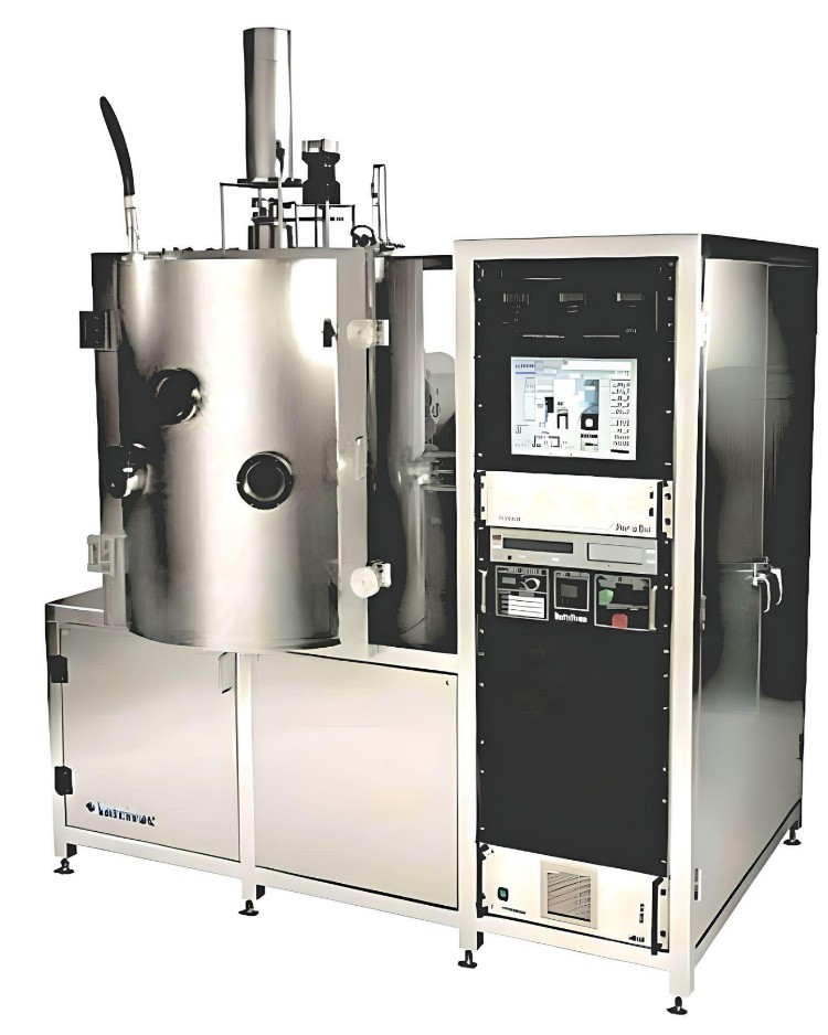
Nanochrome II Thin Film Deposition
- PVD platform in evaporation or sputter configurations
- E-beam and thermal evaporation with ion assist
- Multi-cathode pulsed DC magnetron sputtering
- Substrate heating options up to 800°C
- In-situ stress monitoring on the sputter version
-
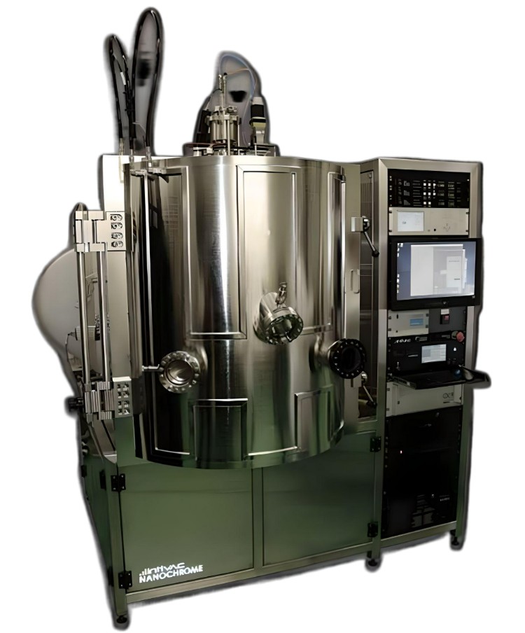
Nanochrome IV UV VIS Thin Film Deposition
- Dual-Axis Rotation for Enhanced Uniformity
- Real-Time Optical Monitoring
- Operator-Friendly Design
- Cutting-Edge Cryopump Technology
- Exceptional Process Repeatability With A Baseline Uniformity Of 2%
-
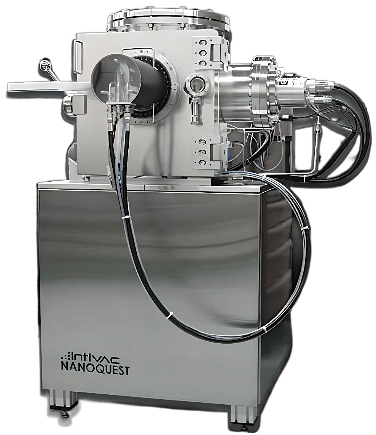
Nanoquest Pico Ion Beam Etch & Milling
- Compact ion milling in a 14″ D-shaped chamber
- Substrates up to 100 mm in diameter
- IBE and RIBE processes
- 1 cm to 8 cm DC, or 4 cm RF ICP ion sources
- Actively cooled, rotating substrate holder
-
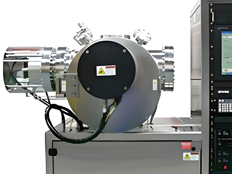
Nanoquest I Ion Beam Etch & Milling
- Ion beam etching of wafers up to 6 inches
- Independent control of ion energy, current density and angle
- Computer-controlled incidence angle, 0° to 270°
- Optional load lock: 1×10⁻⁶ Torr in under 30 minutes
- CAIBE, IBAD and ion beam sputter deposition
-
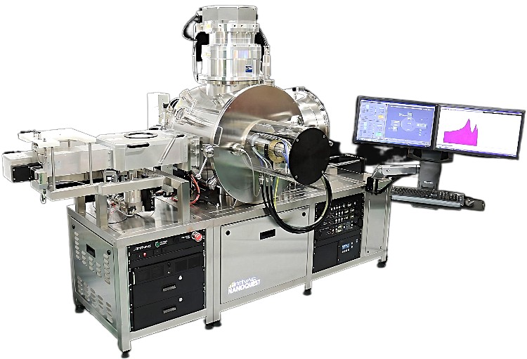
Nanoquest II Ion Beam Etch & Milling
- 22 cm RF ICP ion source, above 1 A
- ±3% uniformity over 100 mm, ±2% wafer to wafer
- Water-cooled stage: 0 to 30 rpm, ±90° tilt
- SIMS end point detection to ±5 Å
- Load lock microscope camera, features to 1 µm
-
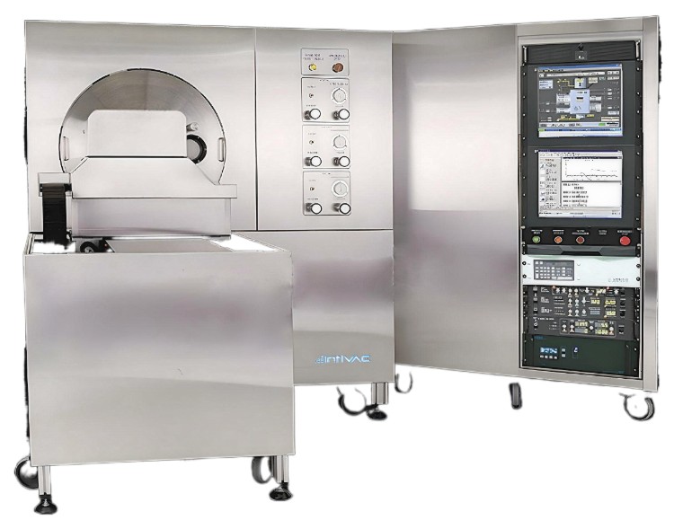
Nanoquest III/IV Ion Beam Etch & Milling
- Batch ion beam etching on up to three platens
- Water-cooled, double-axis planetary stage
- 22 cm RF ion source: above 1 A, 100 to 1500 eV
- Optional SIMS end point detection
- PLC control through a LabVIEW interface
-
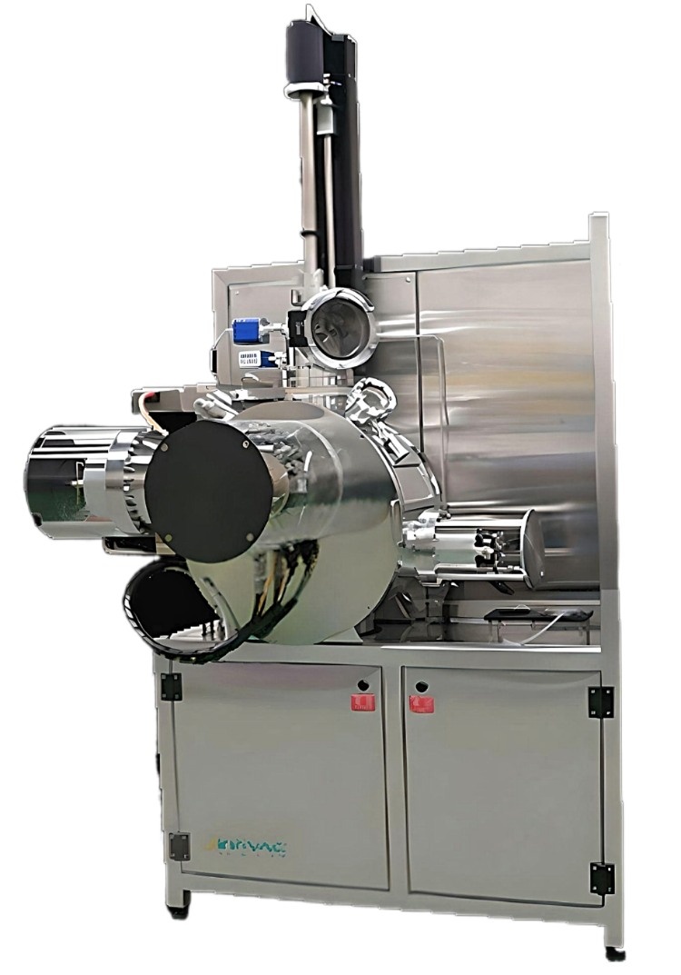
Nanoquest I Combo Ion Beam Sputter Deposition & Etch
- Superior PVD Deposition Capability
- Multi-Target Carousel and Water-Cooled Stage
- Full Ion Beam Etch Capability
- Compact Design with Reputable Coatings
-
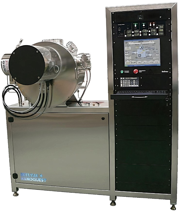
Nanoquest I Ion Beam Sputter Deposition
- Versatile Deposition Capabilities
- Multi-Target Carousel
- Precision Substrate Handling
- Empowering Ion Assist Capability
- Compact Design, Premium Results
-
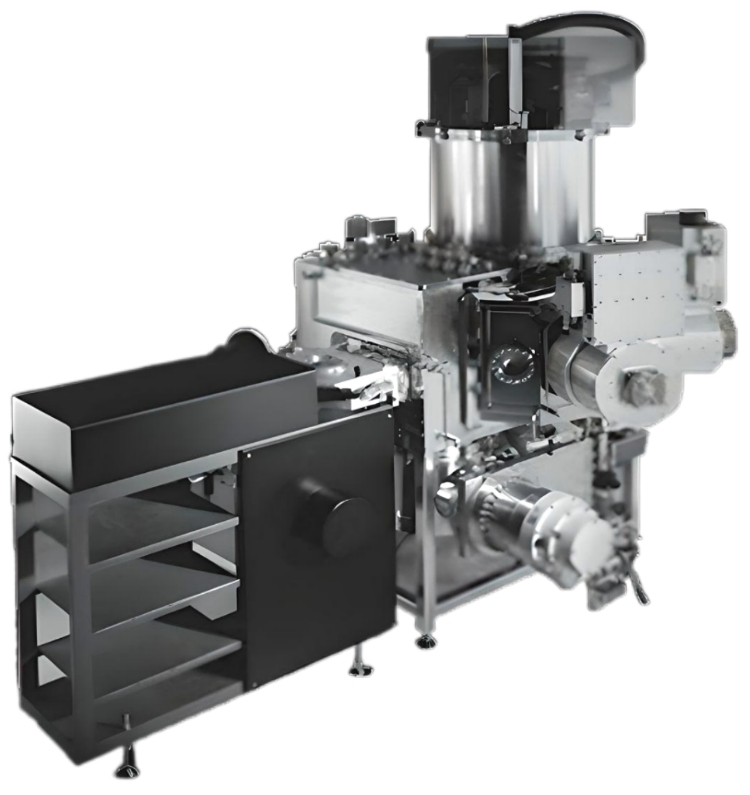
Nanoquest II Ion Beam Sputter Deposition
Superior PVD Deposition Capability
Large Multi-Target Carousel
Rotating and Angle-Tilt Substrate Stage
Ion Assist Capability and Monitoring
High-Density Coatings with Low Particle Levels
-
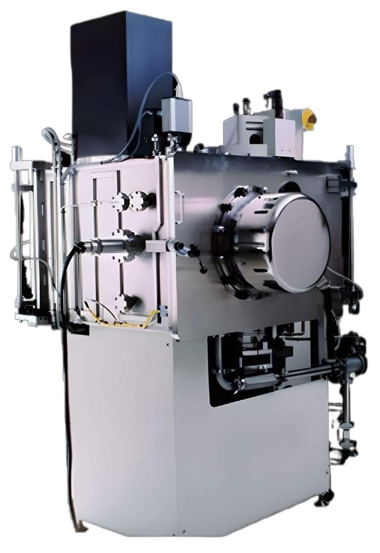
Nanoquest III Ion Beam Sputter Deposition
- Superior PVD Deposition Capability
- Efficient Batch Processing
- Multi-Target Carousel and Planetary Double Rotation
- Angle-Tilt Substrate Stage and Ion Assist Capability
- High-Density Coatings with Low Particles
-
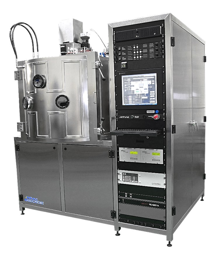
Nanochrome IV Ion Beam Sputter Deposition
- Superior Sputter Up Geometry
- Configurable for Various Loading Options
- Multi-Target Carousel and High-Speed Substrate Stage
- Ion Assist Capability and QCM Instrumentation
- Dynamic Optical Control for Optical Applications