

- Compact ion milling in a 14″ D-shaped chamber
- Substrates up to 100 mm in diameter
- IBE and RIBE processes
- 1 cm to 8 cm DC, or 4 cm RF ICP ion sources
- Actively cooled, rotating substrate holder
Ion Beam Etching and Ion Beam Milling
Ion beam etching (IBE), also called ion milling, removes material by firing a broad, neutralised beam of inert gas ions, usually argon, at the substrate. Removal is physical, so it works on noble metals, magnetic and superconducting films, insulators, diamond films and lithium niobate, all of which are hard to etch chemically. Intlvac Thin Film builds the Nanoquest range of ion beam etch and milling systems, and SiSTEM is Intlvac’s partner for the UK, Ireland and most of Europe.
How ion beam etching works
The ion source sits apart from the substrate, so the beam’s settings can each be set independently: ion energy, ion current density and the angle at which the beam strikes the surface. Rotating and tilting the substrate during the etch keeps it even across the wafer, controls sidewall angle, and clears material that would otherwise redeposit on sidewalls. Etching through photoresist or a hard mask transfers a pattern into the layers below.
IBE, RIBE and CAIBE
Plain IBE uses an inert gas and relies on physical sputtering alone. Reactive ion beam etching (RIBE) adds a reactive gas to the beam, and chemically assisted ion beam etching (CAIBE) introduces it near the substrate. Both add a chemical component, which changes how fast one material etches relative to another and helps with selectivity on mixed stacks.
End-point detection
Secondary ion mass spectrometry (SIMS) reads the material being sputtered as the etch runs, so a process can stop at an interface. On the Nanoquest II, the SIMS end-point system resolves to ±5 Å.
Where it’s used
Intlvac’s systems are used for:
- MEMS and sensors
- photonic waveguides and lithium niobate devices
- magnetic and spintronic films, and data storage
- quantum computing components
- IC delayering and failure analysis
For lithium niobate, DLC hard masks from the Aegis give 4:1 or better selectivity on the Nanoquest II.
Choosing a Nanoquest system
- Nanoquest Pico: compact ion milling in a 14″ D-shaped chamber, for substrates up to 100 mm, with 1 cm to 8 cm DC or 4 cm RF ICP ion sources.
- Nanoquest I: a development platform for wafers up to 6 inches, with a computer-controlled incidence angle from 0° to 270° and an optional load lock. It also runs CAIBE and ion beam deposition.
- Nanoquest II: a 22 cm RF ICP source above 1 A, ±3% uniformity over 100 mm, SIMS end-point detection and a load lock microscope camera.
- Nanoquest III/IV: batch etching on up to three platens, on a water-cooled, double-axis planetary stage.
- Nanoquest I IBSD Combo: deposition and etch on one platform, for substrates up to 100 mm.
Working with SiSTEM
SiSTEM is Intlvac’s partner for the UK, Ireland and most of Europe. We scope your system with you and Intlvac’s engineers, and stay your local contact through quotation, installation and after-sales. Tell us your substrate sizes and the materials you need to etch, and we’ll take it to Intlvac.
Ion Beam Etching (IBE) and Ion Beam Milling (IBM) Tools
-
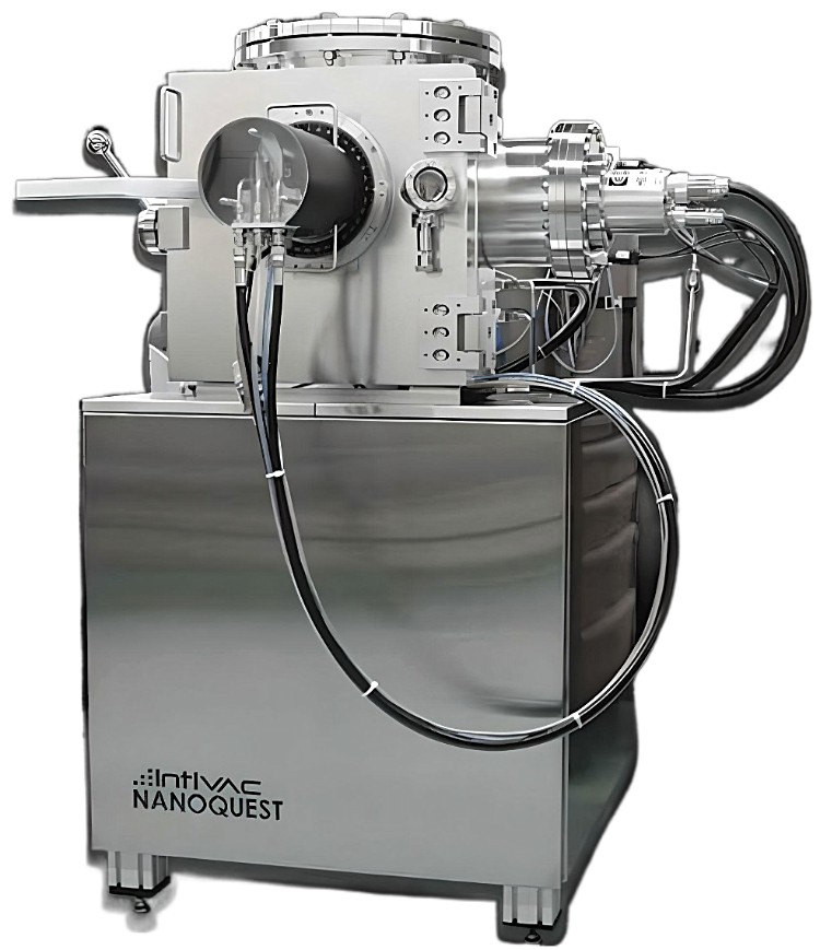
Nanoquest Pico Ion Beam Etch & Milling
-
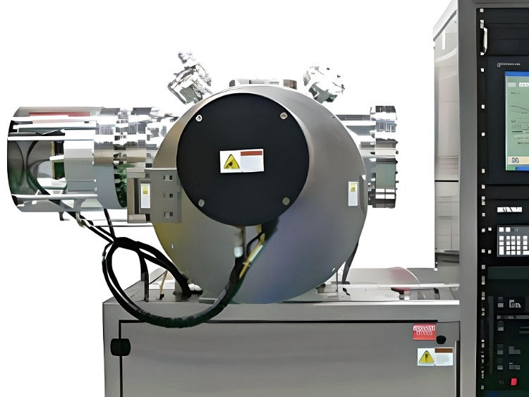
Nanoquest I Ion Beam Etch & Milling
- Ion beam etching of wafers up to 6 inches
- Independent control of ion energy, current density and angle
- Computer-controlled incidence angle, 0° to 270°
- Optional load lock: 1×10⁻⁶ Torr in under 30 minutes
- CAIBE, IBAD and ion beam sputter deposition
-
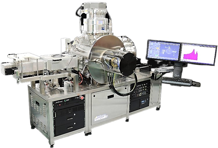
Nanoquest II Ion Beam Etch & Milling
- 22 cm RF ICP ion source, above 1 A
- ±3% uniformity over 100 mm, ±2% wafer to wafer
- Water-cooled stage: 0 to 30 rpm, ±90° tilt
- SIMS end point detection to ±5 Å
- Load lock microscope camera, features to 1 µm
-
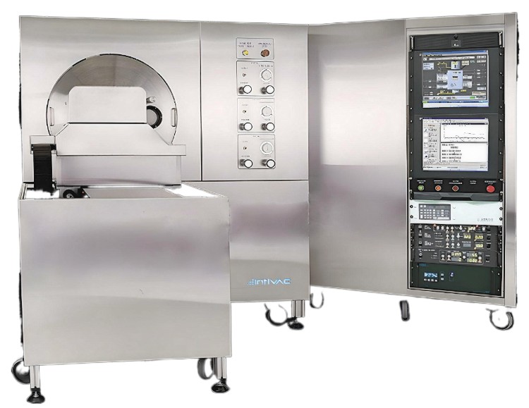
Nanoquest III/IV Ion Beam Etch & Milling
- Batch ion beam etching on up to three platens
- Water-cooled, double-axis planetary stage
- 22 cm RF ion source: above 1 A, 100 to 1500 eV
- Optional SIMS end point detection
- PLC control through a LabVIEW interface
-
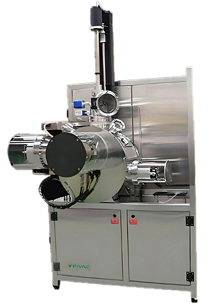
Nanoquest I Combo Ion Beam Sputter Deposition & Etch
- Superior PVD Deposition Capability
- Multi-Target Carousel and Water-Cooled Stage
- Full Ion Beam Etch Capability
- Compact Design with Reputable Coatings