

Why wafers are temporarily bonded
Many devices are made on wafers far thinner than they start. Power devices, RF chips, LEDs, lasers, MEMS and 3D-stacked memory all benefit from a thin substrate: less heat to remove, lower electrical resistance, shorter through-wafer connections or a thinner package. But a wafer thinned below about 100 µm is fragile and flexible, and it can’t be handled, clamped or processed safely on its own. Temporary bonding solves this by fixing the device wafer to a rigid carrier for the thinning and backside steps, then releasing it at the end.
Where it’s used
- Power devices on silicon carbide and silicon, where thinning cuts on-resistance and improves heat flow. In one published silicon carbide example, thinning from 370 to 90 µm reduced on-resistance by more than 30%.
- RF and compound semiconductor devices on gallium arsenide, indium phosphide and gallium nitride, which are brittle and expensive, so every broken wafer counts.
- Through-silicon vias and 3D integration, where the wafer is thinned to expose the vias.
- MEMS and sensors that need backside processing.
Thinning targets range from around 100 µm down to 5 µm or less for some 3D work.
The process, step by step
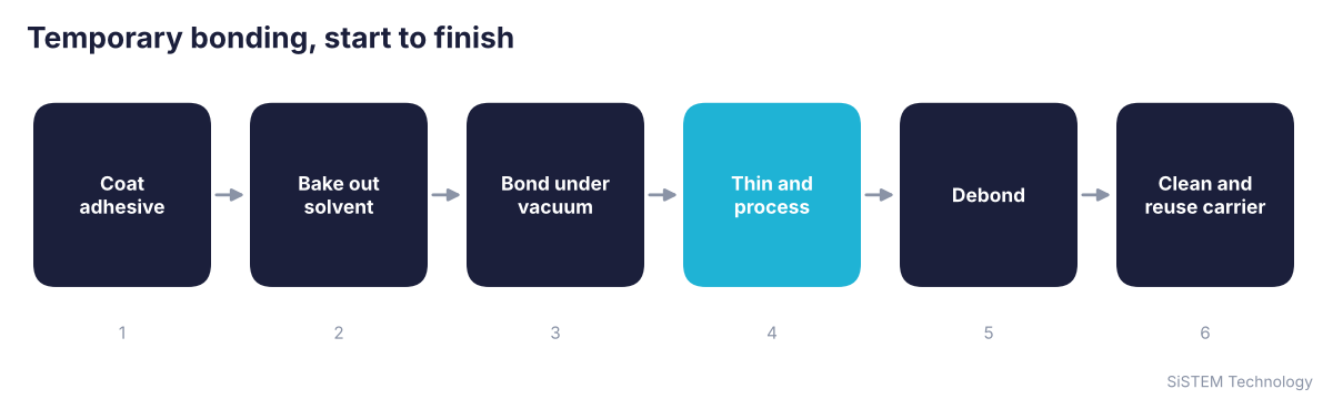
- Coat the adhesive. A temporary adhesive is spin coated onto the device wafer, the carrier or both.
- Bake. A staged bake, typically somewhere between about 120 and 180°C, drives out solvent so it can’t form voids later.
- Bond. The two wafers are aligned and pressed together under vacuum and heat, then cooled slowly.
- Thin and process. The bonded pair goes through grinding, polishing, etching, deposition and lithography on the backside as if it were a thick wafer. Trimming 0.5 to 1 mm from the device wafer edge before grinding reduces chipping.
- Debond. The thinned wafer is released from the carrier, usually onto a film frame or a support, by heat, mechanical peeling, laser or solvent.
- Clean. Adhesive residue is removed from the device wafer, and the carrier is cleaned for reuse.
What makes a good temporary bond
- It holds firmly through every process step, including the highest temperature and the harshest chemistry the wafer will see.
- It’s thin and uniform, so the thinned wafer ends up flat. Total thickness variation (TTV) targets are often below a few microns.
- It’s free of voids, which cause thin spots and cracking during grinding.
- It releases cleanly, without damaging the thin wafer or leaving residue that’s hard to remove.
Choosing the adhesive and carrier is covered in our guide to adhesives and carriers. The ways of separating the wafers are compared in our guide to debonding methods.
How SiSTEM can help
CEE’s temporary bonding and debonding tools cover the whole flow: the Apogee Temporary Bonder, the Apogee Thermal Slide Debonder and the Mechanical Debonder, with Apogee spin coaters and bake plates for the adhesive and spin developers for cleaning. They’ve been qualified with silicon carbide, gallium nitride, gallium arsenide, indium phosphide, sapphire, silicon and glass wafers. Tell us your wafers and process, and we’ll work through it with CEE.