

Debonding methods compared: thermal slide, mechanical, laser and solvent
Getting a thinned wafer off its carrier is the riskiest step in temporary bonding. The wafer is at its thinnest and most valuable, and a crack now loses all the work that came before. There are four main ways to debond, and the choice is usually made at the start, because it decides the adhesive and the carrier.
Thermal slide
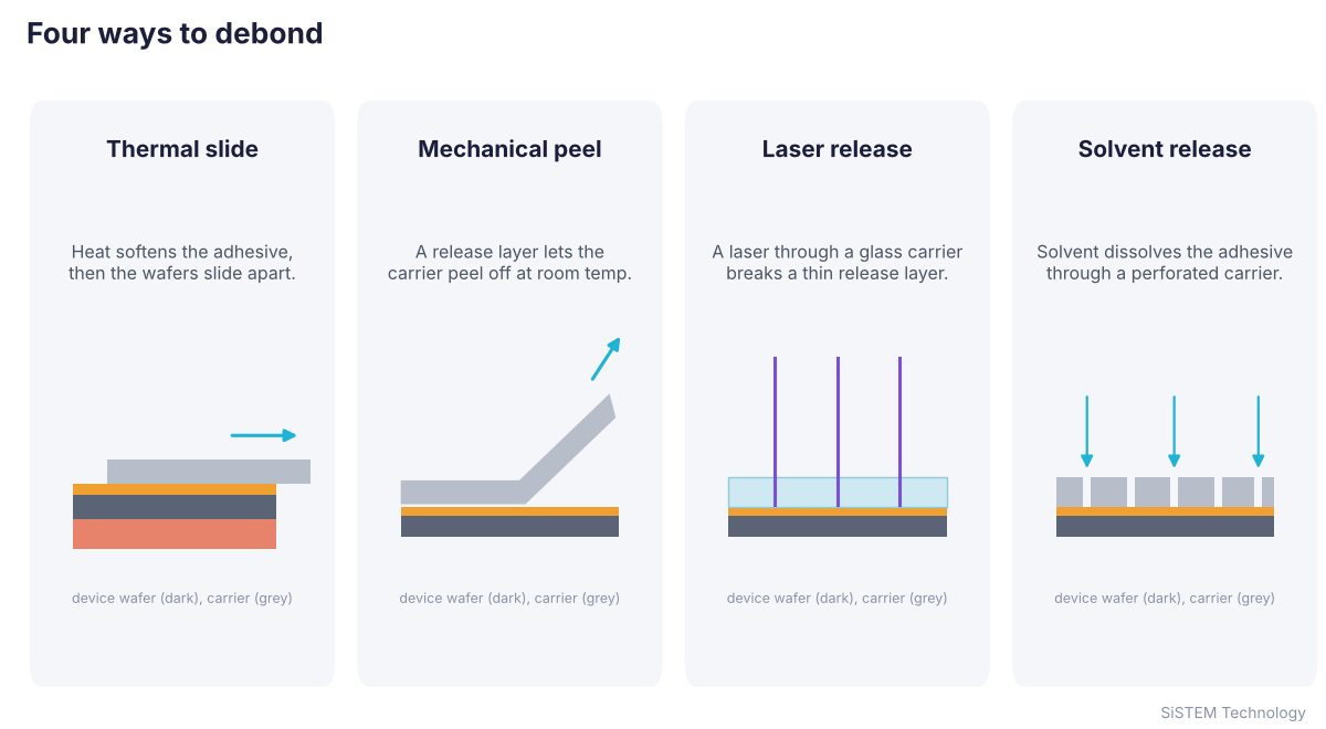
The bonded pair is heated until a thermoplastic adhesive softens, then the device wafer is slid sideways off the carrier while vacuum holds both. It was the first debond method used in volume production and remains widely used.
- Suits: thermoplastic adhesives and waxes, any carrier material.
- Limits: the adhesive must soften at a temperature the devices can tolerate, so it also sets the maximum process temperature. The sliding motion stresses very thin wafers, so speed and force need careful control.
Mechanical peel
A release layer is built into the stack. At room temperature, the carrier is peeled away from the device wafer, which is held on a film frame. There’s no heating at debond.
- Suits: high-temperature processes and curable adhesives, wafers that mustn’t be reheated.
- Limits: needs a suitable release layer, and the peel force must be controlled so it doesn’t crack the wafer.
Laser release
A laser passes through a glass carrier and breaks down a thin release layer, typically about a micron thick, so the carrier lifts off with almost no force. UV wavelengths such as 248, 308 or 355 nm are used.
- Suits: high-volume production, very thin wafers, high-temperature adhesives. Throughput can exceed 30 wafers an hour.
- Limits: needs a glass carrier and a laser-sensitive release layer, and it has the highest equipment cost.
Solvent release
Solvent dissolves the adhesive, reaching it through holes in a perforated carrier or from the edge.
- Suits: low-stress release with simple equipment and the lowest cost.
- Limits: slow, especially on large wafers, and needs perforated carriers or long soaks.
At a glance
| Method | Temperature at debond | Carrier | Stress on wafer | Speed | Cost |
|---|---|---|---|---|---|
| Thermal slide | Raised | Any | Moderate | Moderate | Low to moderate |
| Mechanical peel | Room temperature | Any, with release layer | Low to moderate | Fast | Moderate |
| Laser | Room temperature | Glass | Very low | Fastest | Highest |
| Solvent | Room temperature | Perforated | Very low | Slow | Lowest |
After the debond
Whichever method you use, the device wafer still carries adhesive residue. It’s usually removed with solvent, by soak or spray. A spin developer with solvent spray does this one wafer at a time, rinses and dries under one recipe, and avoids handling the thin wafer through a bath.
How SiSTEM can help
CEE make the Apogee Thermal Slide Debonder, which heats to 300°C and slides wafers apart with 1 to 100 N of controlled force, and the Mechanical Debonder, which peels carriers from 50 to 200 mm wafers on film frames with 1 to 75 N of peel force. Both have been qualified with silicon carbide, gallium nitride, gallium arsenide, indium phosphide, sapphire, silicon and glass. Our temporary bond and debond page compares them. Tell us your adhesive and wafers, and we’ll recommend a debond method with CEE.