- Impressive System Capacity
- Advanced Evaporation Source
- Versatile Wafer Handling
- Automatic Load-Lock for Efficiency
- Wide Range of Applications
Email: info@sistemtechnology.com Call: +44 (0)1327 362 844
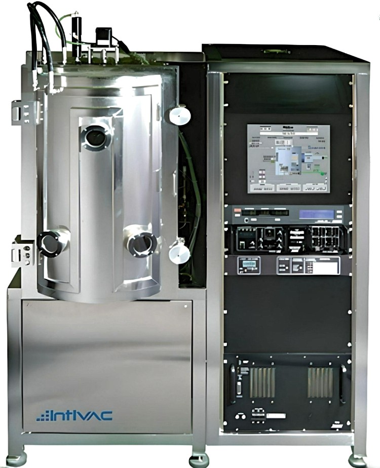
Intlvac: Thin Film Deposition Experts
Intlvac Thin Film Corporation, a prestigious global provider of thin film deposition systems, has earned a reputation for its dedication to advancing vacuum process technology. With headquarters in Delanson, New York, and manufacturing facilities in Canada, Intlvac Thin Flim has been diligently serving a diverse array of industries since its inception in 1963.
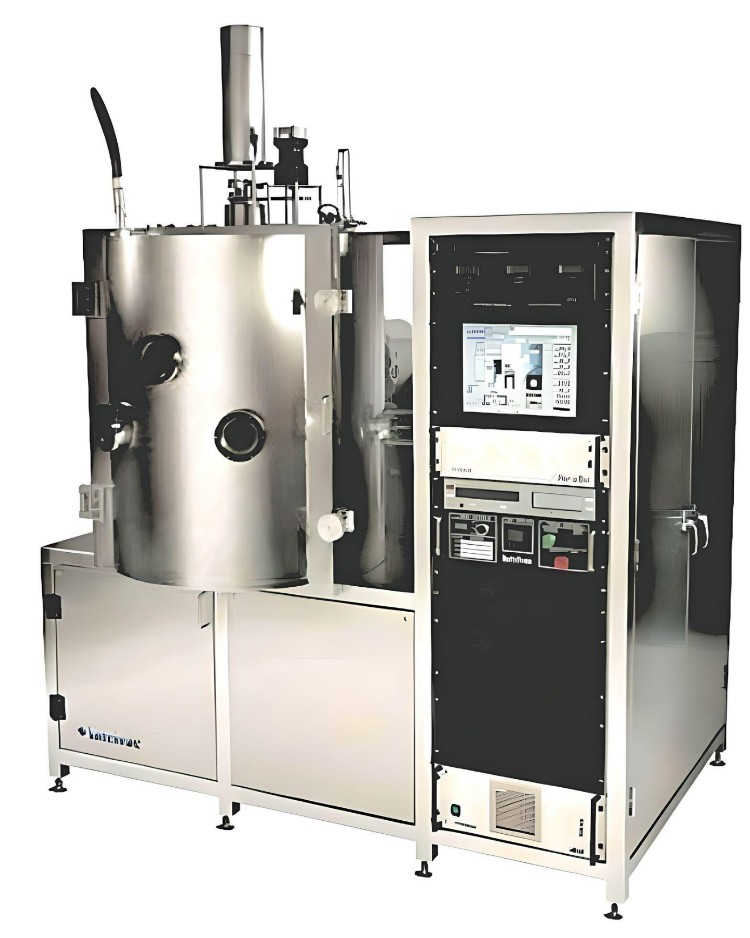
Specialising in the design and manufacture of Ion Beam Etching (IBE), Ion Beam Sputtering (IBS), and Plasma-Enhanced Chemical Vapour Deposition (PECVD) systems, the company caters to the unique needs of sectors such as photonics, aerospace, electronics, and research & development.
Intlvac’s commitment to innovation, coupled with their extensive engineering expertise, has positioned the company as a reliable partner for clients seeking custom-tailored solutions for their thin film deposition requirements. By consistently delivering high-quality equipment and excellent customer service, Intlvac Thin Film Corporation continues to push the boundaries of material science and contribute to the evolution of next-generation technologies.
Customised Solutions
Intlvac Thin Film offers customised solutions to meet the specific needs of its customers. They work closely with their customers to develop tailored solutions that meet their unique requirements and goals.Advanced Technology
Intlvac Thin Film is known for its advanced technology and innovative solutions. They use the latest technologies such as sputtering, evaporation, and ion beam deposition to create high-performance thin films for a range of applications.High Quality
Intlvac Thin Film products are built to last, with high-quality materials and components that are designed for durability and reliability. They have strict quality control processes in place to ensure that each product meets or exceeds industry standards.Technical Support
Intlvac Thin Film provides excellent technical support to its customers, including installation, training, and ongoing support. Their team of experienced engineers and technicians is available to help customers with any issues they may encounter.Energy Efficiency
Intlvac Thin Film products are designed with energy efficiency in mind, helping customers reduce their energy costs and minimize their environmental impact.Cost-Effective
Intlvac Thin Film products are cost-effective, providing customers with high-performance vacuum deposition systems at a competitive price. This makes Intlvac Thin Film products an excellent value proposition for a wide range of industries.Products from Intlvac
-
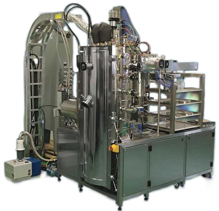
Icarus Indium Deposition System
-
Aegis Diamond-Like Carbon Deposition
- Unleash the Power of DLC
- Unrivalled Precision and Control
- Efficiency Redefined
- Reliability at Its Core
- Innovation in Design
-
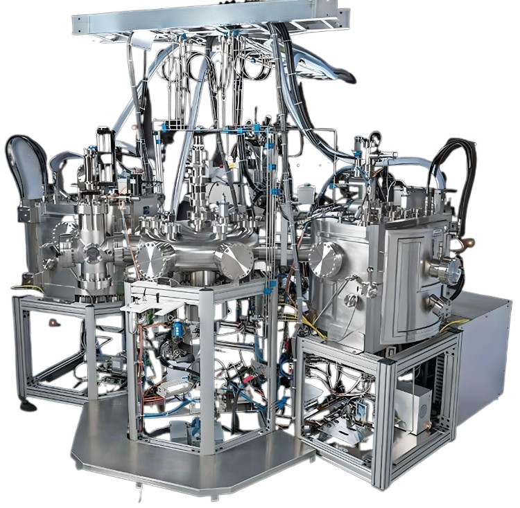
Pleiades Cluster System
- Versatile Cluster System Capabilities: Ion Beam Etching & Sputtering, Atomic Layer Deposition, Thermal Evaporation, eBeam Evaporation – Lift Off, Magnetron Sputtering Metals, Oxide & Fluoride Evaporation, Magnetron Sputtering Oxides & Nitrides
- Customisable Heating and Cooling Options
- Superior Temperature Control for Optimal Results
-
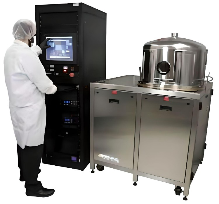
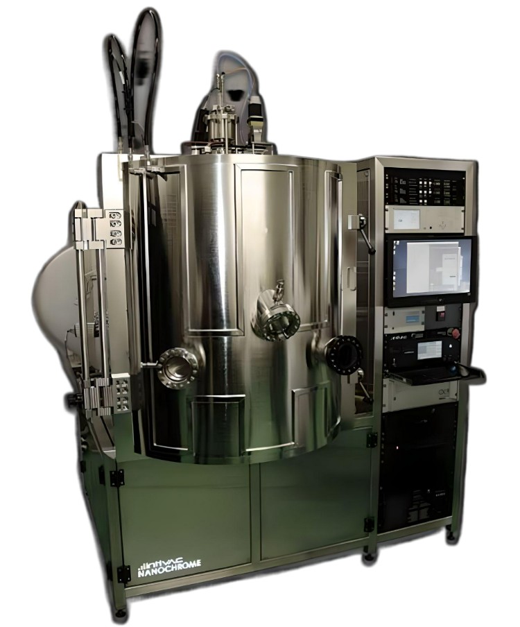
Nanochrome Pico Thin Film Deposition
- Flexible Configuration for Diverse Applications
- Compact Design with Easy Reconfiguration
- Load-Lock Transfer Capability
-
Nanochrome I Thin Film Deposition
- Multi-Layer Deposition and More
- Advanced Electron Beam Evaporation
- Direct Water-Cooled Rotating Substrate Stage
- Automatic Variable Angle Deposition
- Unlock Versatile Thin Film Deposition
-
Nanochrome II Thin Film Deposition
- Explore a Wealth of Deposition Options
- Clamshell Design for Enhanced Access
- Advanced Ion Sources for Enhanced Coating
- Tailored Fixturing for Uniform Coatings
- High Vacuum Efficiency
- High-Quality Construction for Optimal Performance
- Versatile Feedthrough Ports and Optical Window
-
Nanochrome IV UV VIS Thin Film Deposition
- Dual-Axis Rotation for Enhanced Uniformity
- Real-Time Optical Monitoring
- Operator-Friendly Design
- Cutting-Edge Cryopump Technology
- Exceptional Process Repeatability With A Baseline Uniformity Of 2%
-
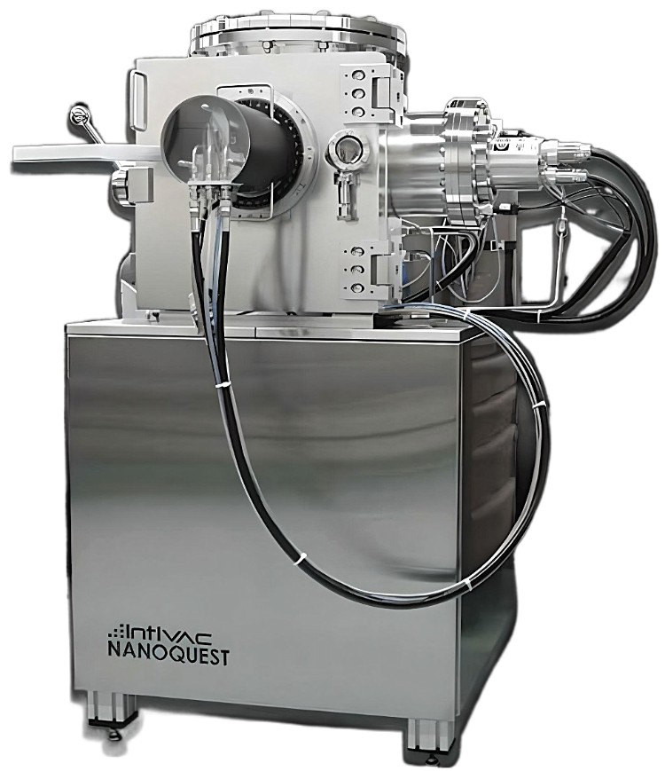
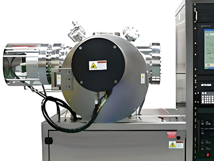
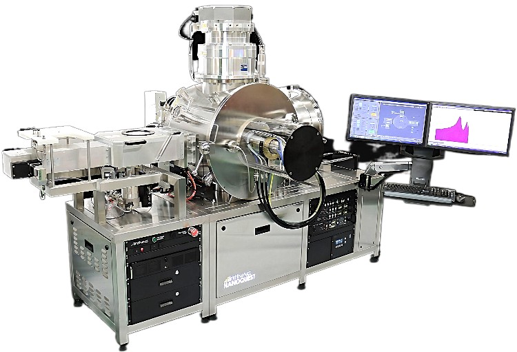
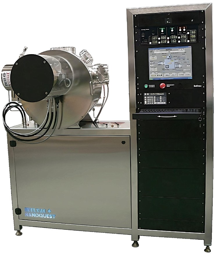
Nanoquest Pico Ion Beam Etch & Milling
- Precision Ion Beam Etching
- Fast Pumping and Ultimate Pressure
- Flexible Substrate Fixturing
- Wide Substrate Size Compatibility
- Comprehensive Ion Milling Capabilities
- Expansion Options
-
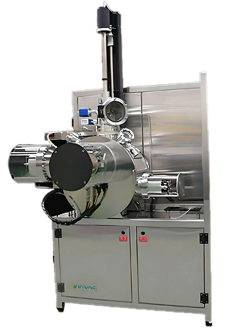
Nanoquest I Ion Beam Etch & Milling
- Compact Design, Uncompromised Performance
- Automated Excellence
- Enhanced Efficiency with Nanoquest I-LL (Load Lock) System
- Versatile Chamber Design
- Flexible Configurations for Maximum Potential
- Experience the Power of Precision
-
Nanoquest II Ion Beam Etch & Milling
- Advanced Nanofabrication Capabilities
- Flexible Configuration Options
- High-Performance Wafer Handling
- Atomic Layer Etching Capabilities
-
Nanoquest III/IV Ion Beam Etch & Milling
- Efficient Batch Processing
- Advanced Water-Cooled Double Axis Stage
- Wide Process Range
- RF Ion Source and Endpoint Detection
- Intuitive Operation and Display
- Experience Precision and Versatility
-
Nanoquest I Combo Ion Beam Sputter Deposition & Etch
- Superior PVD Deposition Capability
- Multi-Target Carousel and Water-Cooled Stage
- Full Ion Beam Etch Capability
- Compact Design with Reputable Coatings
-
Nanoquest I Ion Beam Sputter Deposition
- Versatile Deposition Capabilities
- Multi-Target Carousel
- Precision Substrate Handling
- Empowering Ion Assist Capability
- Compact Design, Premium Results
-
Nanoquest II Ion Beam Sputter Deposition
Superior PVD Deposition Capability
Large Multi-Target Carousel
Rotating and Angle-Tilt Substrate Stage
Ion Assist Capability and Monitoring
High-Density Coatings with Low Particle Levels
-
Nanoquest III Ion Beam Sputter Deposition
- Superior PVD Deposition Capability
- Efficient Batch Processing
- Multi-Target Carousel and Planetary Double Rotation
- Angle-Tilt Substrate Stage and Ion Assist Capability
- High-Density Coatings with Low Particles
-
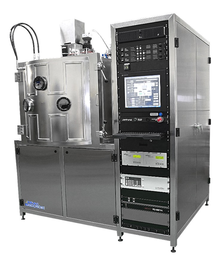
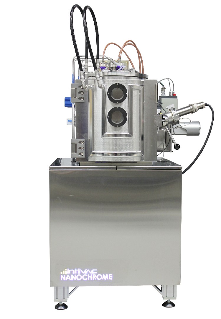
Nanochrome IV Ion Beam Sputter Deposition
- Superior Sputter Up Geometry
- Configurable for Various Loading Options
- Multi-Target Carousel and High-Speed Substrate Stage
- Ion Assist Capability and QCM Instrumentation
- Dynamic Optical Control for Optical Applications
-
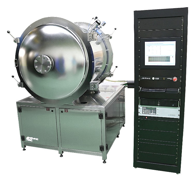
Deimos - TVAC1
- State-Of-The-Art Thermal Vacuum Testing System
- Unparalleled Control and Reliability
- Simulate Space Vacuum Conditions
- Wide Temperature Range for Comprehensive Testing
- Enhanced Safety and Operational Control
-
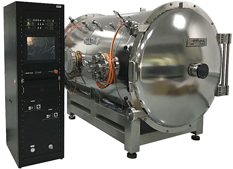
Phobos TVAC2 - Thermal Vacuum Chamber
- Unparalleled Control and Reliability
- Simulation of Space and Thermal Conditions
- High Vacuum and Clean Testing Environment
- Advanced Control and Monitoring
-
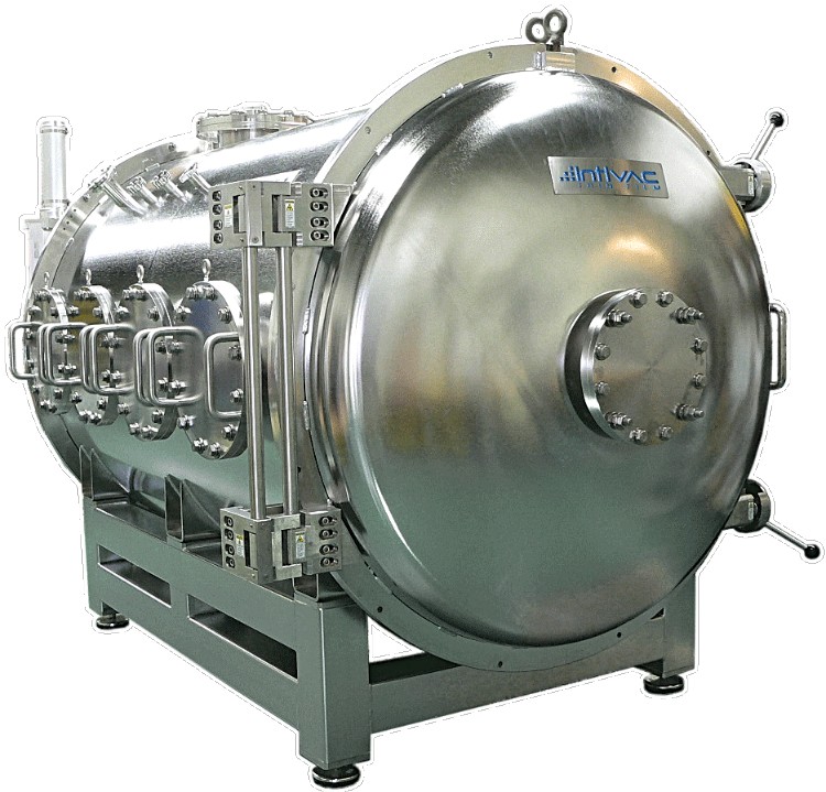
Ares - TVAC3 Thermal Vacuum Chamber
- Precise Thermal Cycling Under High Vacuum
- Oil-Free High Vacuum Pumping
- Efficient Temperature Cycling
- Intuitive Controls and Monitoring
- Reliable and Safe Operation
-
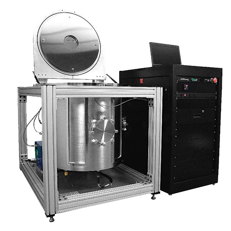
Aether Vacuum Degassing
- Unleash the Power of Degassing
- Unrivalled Precision and Control
- Efficiency Redefined
- Reliability at Its Core
- Innovation in Design